ADC1 Register Reference Chapter
Official register map, bit fields, and the modeled PA1 / CURRENT_SENSE path
ADC User Description: TIM2 event, EOC, and ADC1_2 interrupt route
Contents
- General description
- Main features
- Reference figures and tables
- Official ADC1 register map
- Modeled register descriptions
- Trainer contract and legacy boundary
1 General description
ADC1 converts an analog input voltage into a 12-bit digital result. The ADC path is GPIO analog input -> ADC_SQR3-selected Analog MUX -> Sample & Hold -> ADC converter -> ADC_DR, with status and transfer helpers such as EOC, DMA, and Analog watchdog around that path.
A GPIO pin is the physical analog pad, while the ADC channel number is the selector value that tells the regular sequencer and Analog MUX which input to forward. For example, PA1 maps to ADC1_IN1, while other package pins map to different ADC channel numbers. The channel selection logic controls the MUX; it is not another signal-processing stage after it.
In the current motor-driver trainer lab, PA1 carries the CURRENT_SENSE signal. That fixed implemented route is separate from full STM32-style multiplexed channel coverage.
2 Main features
2.1 Official STM32-style concepts
- 12-bit unsigned conversion result, 0 .. 4095
- Official STM32F103 analog input range: 0 V .. VREF+; VREF+ ≤ VDDA, with VDDA = 2.4 V .. 3.6 V
- Regular conversion, single-shot, continuous mode, and scan mode
- Channel order configured through ADC_SQR1 and ADC_SQR3
- Sample time configured through ADC_SMPR1 and ADC_SMPR2
- End-of-conversion status in ADC_SR.EOC
- DMA request support and analog watchdog thresholds
- Temperature sensor and VREFINT internal channels
2.2 Currently simulated subset
- Fixed implemented channel for PA1 / ADC1_IN1 / CURRENT_SENSE
- Official-layout regular path through ADC_SQR3, ADC_CR1/CR2, ADC_SR, and ADC_DR
- TIM2_CC2 trigger, EOC, ADC1_2 interrupt, and DR-read EOC clear behavior
- Private ADC1_CR/DR_CH0/DR_CH1 aliases retained only for legacy lessons; PB0 channel 8 and selectable PA6 channel 6 use the official regular path
- Common PA1 / CURRENT_SENSE uses the Trainer's 3.3 V ADC reference: 0.0 V .. 3.3 V maps to 0 .. 4095
- GPIO analog-input setup should still be taught for realism through GPIOA->CRL
3 Reference figures and tables
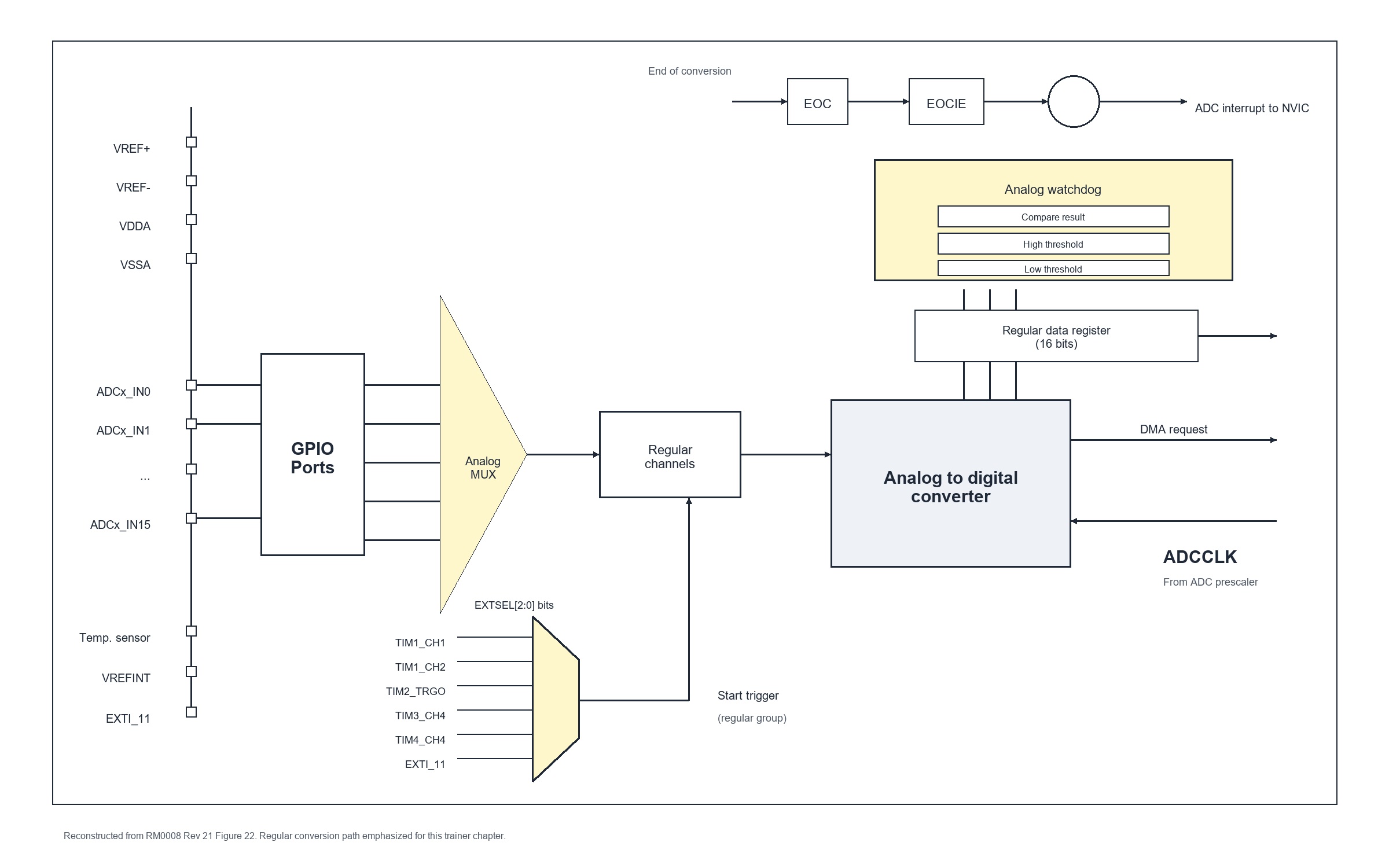
Figure 1. Reconstructed ADC regular-conversion path based on RM0008 Figure 22
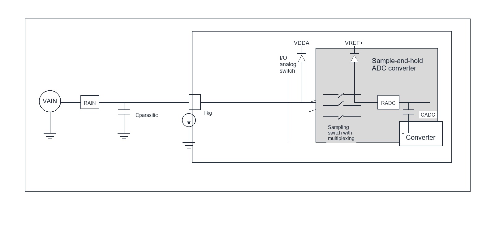
Figure 2. Reconstructed ADC input equivalent circuit based on DS5319 Figure 38
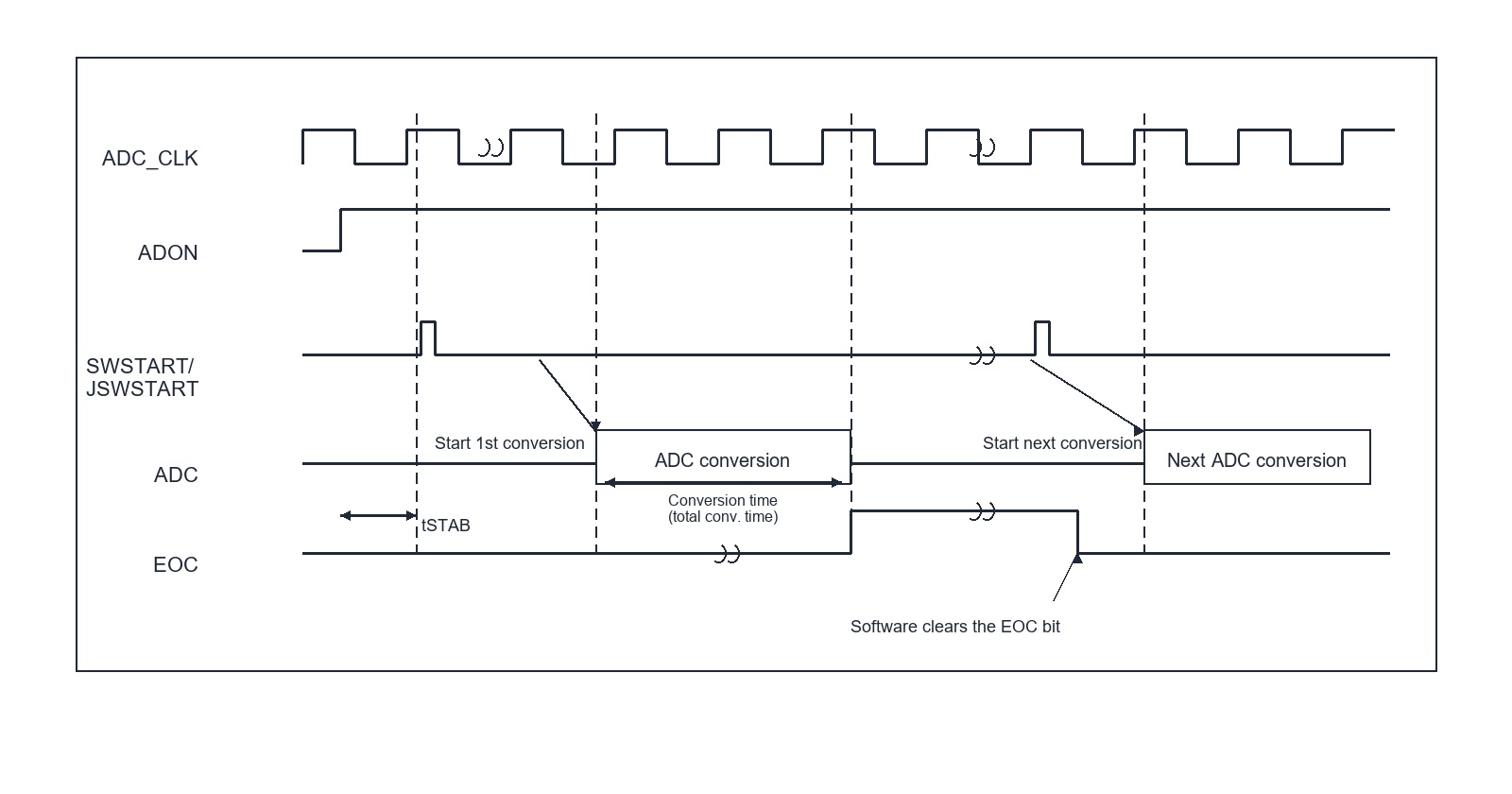
Figure 3. Reconstructed regular conversion timing based on RM0008 Figure 23
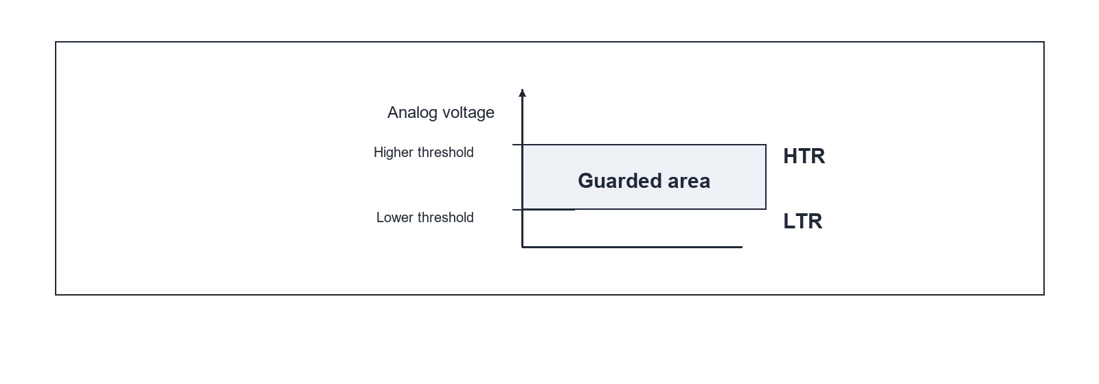
Figure 4. Reconstructed analog watchdog guarded area based on RM0008 Figure 24
| Table 1. Pin mapping examples used in this chapter | ||
|---|---|---|
| Signal source | ADC channel | Meaning |
| PA1 | ADC1_IN1 | External analog input pin; current trainer route is CURRENT_SENSE |
| PA6 | ADC1_IN6 | Selectable AS5600 analog absolute-angle input. The common hardware profile is 3.3 V mode, OUTS=00, and programmed MANG=180°; official STM32F103 pin tables name this pad function ADC12_IN6. |
| PB0 | ADC_IN8 | Independent NTCLE100E3103 temperature divider node: 3.3 V → R1 10 kΩ → PB0 → NTC → GND |
| PB1 | ADC_IN9 | Official STM32 ADC input; not connected by the current System Trainer harness |
| Temperature sensor | ADC_IN16 | Internal channel, not an external GPIO pad |
| VREFINT | ADC_IN17 | Internal reference channel |
Reference source: STM32F103 Datasheet, p.29, Table 5. Pin definitions. What this table means: GPIO pin names and ADC channel numbers are different concepts. Related registers: ADC_SQRx, GPIOx_CRL, GPIOx_CRH; for the current trainer route, PA1 means GPIOA_CRL[7:4] plus ADC1_IN1.
3.1 PA1, PA6, and PB0 GPIO nibbles before ADC conversion
| Pin / ADC input | GPIO field | 4-bit value | Actual pin behavior | Current trainer result |
|---|---|---|---|---|
| PA1 / ADC1_IN1 | GPIOA_CRL[7:4], shift 4, mask 0x000000F0 | 0x0 (0000): CNF=00, MODE=00 | Analog input. The digital input buffer and output driver are disabled so the ADC can own the pad path. | The PA1 route requires this exact nibble together with IOPAEN, ADC1EN, and ADC_SQR3.SQ1 = 1. |
| PA6 / ADC1_IN6 | GPIOA_CRL[27:24], shift 24, mask 0x0F000000 | 0x0 (0000): CNF=00, MODE=00 | Analog input for the 3.3 V AS5600 OUT voltage. | Feedback=POSITION requires IOPAEN, ADC1EN, PA6 analog mode, and SQ1=6. With local OUTS=00 / MANG=180°, the sensor provides 2048 distinct DAC steps across 0..180°; the STM32 ADC still reports a 12-bit 0..4095 code, so adjacent ADC codes can repeat. |
| PB0 / ADC1_IN8 | GPIOB_CRL[3:0], shift 0, mask 0x0000000F | 0x0 (0000): CNF=00, MODE=00 | Analog input for the NTC divider node. | NTC measurement requires IOPBEN, ADC1EN, PB0 analog mode, and SQ1=8. With R1=10 kΩ and NTCLE100E3103 R25=10 kΩ, the node is 1.65 V and ADC raw is about 2048 at 25 °C. |
Write the PA1 field as GPIOA->CRL &= ~(0xFu << 4), PA6 as GPIOA->CRL &= ~(0xFu << 24), and PB0 as GPIOB->CRL &= ~0xFu. The complete 0x0..0xF mode table and shift calculation are in the GPIO Register Datasheet.
4 Official ADC1 register map
The register block below follows RM0008 Rev 21, Section 11.12 and Table 72. ADC peripheral registers are accessed as 32-bit words. Absolute addresses use ADC1 base 0x40012400 + offset.
| Offset | Absolute address | Register | Reset value | Official purpose | Trainer status |
|---|---|---|---|---|---|
| 0x00 | 0x40012400 | ADC_SR | 0x00000000 | Status flags | EOC modeled |
| 0x04 | 0x40012404 | ADC_CR1 | 0x00000000 | Scan, watchdog, and interrupt control | EOCIE modeled |
| 0x08 | 0x40012408 | ADC_CR2 | 0x00000000 | Trigger, alignment, DMA, calibration, and enable control | ADON / EXTSEL / EXTTRIG / SWSTART modeled; CONT stored only |
| 0x0C | 0x4001240C | ADC_SMPR1 | 0x00000000 | Sample time for channels 10 to 17 | 미지원 |
| 0x10 | 0x40012410 | ADC_SMPR2 | 0x00000000 | Sample time for channels 0 to 9 | Stored/readback only; sample-cycle timing side effect is 미지원 |
| 0x14 | 0x40012414 | ADC_JOFR1 | 0x00000000 | Injected channel 1 data offset | 미지원 |
| 0x18 | 0x40012418 | ADC_JOFR2 | 0x00000000 | Injected channel 2 data offset | 미지원 |
| 0x1C | 0x4001241C | ADC_JOFR3 | 0x00000000 | Injected channel 3 data offset | 미지원 |
| 0x20 | 0x40012420 | ADC_JOFR4 | 0x00000000 | Injected channel 4 data offset | 미지원 |
| 0x24 | 0x40012424 | ADC_HTR | 0x00000FFF | Analog watchdog high threshold | 미지원 |
| 0x28 | 0x40012428 | ADC_LTR | 0x00000000 | Analog watchdog low threshold | 미지원 |
| 0x2C | 0x4001242C | ADC_SQR1 | 0x00000000 | Regular sequence length and slots 13 to 16 | 미지원 |
| 0x30 | 0x40012430 | ADC_SQR2 | 0x00000000 | Regular sequence slots 7 to 12 | 미지원 |
| 0x34 | 0x40012434 | ADC_SQR3 | 0x00000000 | Regular sequence slots 1 to 6 | SQ1 modeled |
| 0x38 | 0x40012438 | ADC_JSQR | 0x00000000 | Injected sequence | 미지원 |
| 0x3C | 0x4001243C | ADC_JDR1 | 0x00000000 | Injected data 1 | 미지원 |
| 0x40 | 0x40012440 | ADC_JDR2 | 0x00000000 | Injected data 2 | 미지원 |
| 0x44 | 0x40012444 | ADC_JDR3 | 0x00000000 | Injected data 3 | 미지원 |
| 0x48 | 0x40012448 | ADC_JDR4 | 0x00000000 | Injected data 4 | 미지원 |
| 0x4C | 0x4001244C | ADC_DR | 0x00000000 | Regular conversion data | 12-bit result modeled |
Source: RM0008 Rev 21, Section 11.12, Table 72. The table keeps the complete official map visible even when a register is not executable in the trainer.
5 Register descriptions
Yellow fields have an active trainer side effect. Blue fields are official fields that remain stored or are shown for register reading. Reserved fields must remain at their reset value.
5.1 ADC status register (ADC_SR)
Address offset: 0x00 Address: 0x40012400 Reset value: 0x00000000
| Bit | Name | Access / values | Meaning | Current trainer register-value behavior |
|---|---|---|---|---|
| 31:5 | Reserved | - | Keep at reset value | - |
| 4 | STRT | rc_w0; 0 = no regular conversion has started, 1 = regular conversion has started | Hardware status flag for regular conversion start. | 미지원 |
| 3 | JSTRT | rc_w0; 0 = no injected conversion has started, 1 = injected conversion has started | Hardware status flag for injected conversion start. | 미지원 |
| 2 | JEOC | rc_w0; 0 = injected conversion not complete, 1 = injected conversion complete | Hardware status flag for injected conversion completion. | 미지원 |
| 1 | EOC | rc_w0; 0 = conversion not complete, 1 = conversion complete | Hardware status flag for regular or injected group conversion completion. | Set when ADC_DR is updated; ADC_DR read clears it |
| 0 | AWD | rc_w0; 0 = no analog watchdog event, 1 = analog watchdog event occurred | Hardware status flag for an analog watchdog threshold event. | 미지원 |
5.2 ADC control register 1 (ADC_CR1)
Address offset: 0x04 Address: 0x40012404 Reset value: 0x00000000
| Bit | Name | Access / values | Meaning | Current trainer register-value behavior |
|---|---|---|---|---|
| 23 | AWDEN | rw; 0 = disabled, 1 = enabled | Watchdog on regular channels | 미지원 |
| 22 | JAWDEN | rw; 0 = disabled, 1 = enabled | Watchdog on injected channels | 미지원 |
| 19:16 | DUALMOD[3:0] | rw; 0000 = independent, 0001..1001 = official dual-ADC modes, 1010..1111 = Reserved | Dual ADC operating mode. STM32F103 medium-density ADC1 trainer uses independent behavior only. | 미지원 |
| 15:13 | DISCNUM[2:0] | rw; 000 = 1 channel, 001 = 2 channels, ..., 111 = 8 channels | Number of regular channels converted in discontinuous mode after an external trigger. | 미지원 |
| 12, 11 | JDISCEN, DISCEN | rw; each bit: 0 = discontinuous mode disabled, 1 = discontinuous mode enabled | Enable injected and regular discontinuous conversion mode. | 미지원 |
| 10 | JAUTO | rw; 0 = automatic injected conversion disabled, 1 = automatic injected conversion enabled | Run injected group conversion automatically after regular group conversion. | 미지원 |
| 9 | AWDSGL | rw; 0 = watchdog on all channels, 1 = watchdog on selected channel | Select whether the analog watchdog watches every channel or the channel named by AWDCH[4:0]. | 미지원 |
| 8 | SCAN | rw; 0 = scan mode disabled, 1 = scan mode enabled | Convert selected ADC_SQRx or ADC_JSQRx sequence entries as a scan. | 미지원 |
| 7, 6 | JEOCIE, AWDIE | rw; each bit: 0 = interrupt disabled, 1 = interrupt enabled | Enable injected-EOC and analog-watchdog interrupt requests. | 미지원 |
| 5 | EOCIE | rw; 0 = disabled, 1 = interrupt enabled | End-of-conversion interrupt enable | EOC와 함께 ADC1_2 handler 요청을 만듭니다. |
| 4:0 | AWDCH[4:0] | rw; 00000..10001 = ADC channel 0..17, 10010..11111 = Reserved | Analog watchdog channel selection. | 미지원 |
5.3 ADC control register 2 (ADC_CR2)
Address offset: 0x08 Address: 0x40012408 Reset value: 0x00000000
| Bit | Name | Access / values | Meaning | Current trainer register-value behavior |
|---|---|---|---|---|
| 23 | TSVREFE | rw; 0 = temperature sensor and VREFINT disabled, 1 = enabled | Enable the internal temperature sensor and VREFINT channel. | 미지원 |
| 22, 21 | SWSTART, JSWSTART | rw; each bit: 0 = reset state, 1 = start the selected regular or injected conversion group | Software start request for regular and injected groups. Hardware clears the bit after conversion starts. | SWSTART executes one PB0/IN8 or PA6/IN6 regular conversion selected by SQ1, then clears; JSWSTART is not modeled |
| 20 | EXTTRIG | rw; 0 = disabled, 1 = external trigger enabled | Enable external trigger for regular group | Required for common TIM2_CC2 current conversion and PB0/PA6 SWSTART conversion |
| 19:17 | EXTSEL[2:0] | rw; see shared decoder below | Select regular-group trigger event | 011 executes TIM2_CC2; 111 selects the PB0/PA6 SWSTART route |
| 15 | JEXTTRIG | rw; 0 = disabled, 1 = enabled | Enable injected external trigger | 미지원 |
| 14:12 | JEXTSEL[2:0] | rw; ADC1/ADC2: 000 = TIM1_TRGO, 001 = TIM1_CC4, 010 = TIM2_TRGO, 011 = TIM2_CC1, 100 = TIM3_CC4, 101 = TIM4_TRGO, 110 = EXTI15/TIM8_CC4, 111 = JSWSTART | Select injected trigger event. | 미지원 |
| 11 | ALIGN | rw; 0 = right alignment, 1 = left alignment | Select ADC_DR data alignment. | Stored; trainer result remains right-aligned |
| 8 | DMA | rw; 0 = DMA mode disabled, 1 = DMA mode enabled | Enable ADC DMA request generation. | 미지원 |
| 3, 2 | RSTCAL, CAL | rw; RSTCAL: 0 = calibration register initialized, 1 = initialize calibration register; CAL: 0 = calibration complete, 1 = start calibration | Reset calibration registers and start A/D calibration. | Stored; calibration timing not modeled |
| 1 | CONT | rw; 0 = single conversion mode, 1 = continuous conversion mode | Continuous conversion mode. | Stored; continuous conversion not modeled |
| 0 | ADON | rw; 0 = ADC disabled and powered down, 1 = ADC enabled; writing 1 again while already enabled starts conversion on hardware | ADC enable and software conversion start sequence. | Common PA1/TIM2_CC2 and PB0/PA6 SWSTART paths require ADON=1; stabilization and repeated-ADON timing are simplified |
Shared ADC_CR2 EXTSEL decoder: the values below are official RM0008 regular-group trigger selections. The trainer execution column is a separate support boundary.
| EXTSEL | Official ADC1/ADC2 regular trigger | Trainer execution |
|---|---|---|
| 000 | TIM1_CC1 | 미지원 |
| 001 | TIM1_CC2 | 미지원 |
| 010 | TIM1_CC3 | 미지원 |
| 011 | TIM2_CC2 | Value 011 executes TIM2_CC2 when ADON=1, EXTTRIG=1, and the ADC/TIM2 route is configured. |
| 100 | TIM3_TRGO | 미지원 |
| 101 | TIM4_CC4 | 미지원 |
| 110 | EXTI11 / TIM8_TRGO | 미지원 |
| 111 | SWSTART | Executes one PB0/IN8 or PA6/IN6 conversion when ADON=1, EXTTRIG=1, SQ1 selects channel 8 or 6, and SWSTART is written. |
5.4 ADC sample time register 2 (ADC_SMPR2)
Address offset: 0x10 Address: 0x40012410 Reset value: 0x00000000
| Field | Name | Access / values | Meaning | Current trainer register-value behavior |
|---|---|---|---|---|
| SMP9[2:0] .. SMP0[2:0] | Sample time fields | rw; 000=1.5, 001=7.5, 010=13.5, 011=28.5, 100=41.5, 101=55.5, 110=71.5, 111=239.5 cycles | Sample time for ADC channels 9 to 0. | Official reference only in the focused trainer API; cycle-accurate timing is simplified |
| SMP1[5:3] | PA1 / ADC1_IN1 | rw; same 3-bit sample-time encoding | Sample time for the trainer's PA1 analog input channel. | Internally stored reference field; no modeled sample-cycle timing side effect |
5.5 ADC regular sequence register 3 (ADC_SQR3)
Address offset: 0x34 Address: 0x40012434 Reset value: 0x00000000
| Field | Name | Access / values | Meaning | Current trainer register-value behavior |
|---|---|---|---|---|
| 29:25 | SQ6[4:0] | rw; channel number | Sixth regular conversion channel. | 미지원 sequence slot |
| 24:20 | SQ5[4:0] | rw; channel number | Fifth regular conversion channel. | 미지원 sequence slot |
| 19:15 | SQ4[4:0] | rw; channel number | Fourth regular conversion channel. | 미지원 sequence slot |
| 14:10 | SQ3[4:0] | rw; channel number | Third regular conversion channel. | 미지원 sequence slot |
| 9:5 | SQ2[4:0] | rw; channel number | Second regular conversion channel. | 미지원 sequence slot |
| 4:0 | SQ1[4:0] | rw; 00000..10001 = ADC channel 0..17, 10010..11111 = Reserved | First regular conversion channel. | Value 00001 selects PA1 / ADC1_IN1 |
5.6 ADC regular data register (ADC_DR)
Address offset: 0x4C Address: 0x4001244C Reset value: 0x00000000
| Field | Name | Access / values | Meaning | Current trainer register-value behavior |
|---|---|---|---|---|
| 31:16 | ADC2DATA[15:0] | ro | ADC2 regular data in dual mode. | 미지원 |
| 15:0 | DATA[15:0] | ro; 0..4095 for a right-aligned 12-bit result, alignment controlled by ADC_CR2.ALIGN | Regular conversion data, left or right aligned by ALIGN. | Right-aligned 12-bit PA1/IN1, PA6/IN6, or PB0/IN8 sample in bits 11:0; read clears EOC |
5.7 Reference-only ADC register field details
These official registers stay in the ADC1 map so students can recognize the complete RM0008 block. They are not exposed as focused trainer fields unless the trainer behavior column says otherwise.
| Register / offset | Name | Access / values | Meaning | Current trainer register-value behavior |
|---|---|---|---|---|
| ADC_SMPR1 / 0x0C | SMP17[2:0]..SMP10[2:0] | rw; same 3-bit sample-time encoding as ADC_SMPR2 | Sample time for channels 10 through 17. | 미지원; channels 10-17 are not routed by the current trainer. |
| ADC_JOFR1 / 0x14 | JOFFSET1[11:0] | rw; 12-bit offset | Injected channel 1 data offset. | 미지원; injected conversions are not modeled. |
| ADC_JOFR2 / 0x18 | JOFFSET2[11:0] | rw; 12-bit offset | Injected channel 2 data offset. | 미지원; injected conversions are not modeled. |
| ADC_JOFR3 / 0x1C | JOFFSET3[11:0] | rw; 12-bit offset | Injected channel 3 data offset. | 미지원; injected conversions are not modeled. |
| ADC_JOFR4 / 0x20 | JOFFSET4[11:0] | rw; 12-bit offset | Injected channel 4 data offset. | 미지원; injected conversions are not modeled. |
| ADC_HTR / 0x24 | HT[11:0] | rw; reset 0xFFF | Analog watchdog high threshold. | 미지원; analog watchdog comparison is not modeled. |
| ADC_LTR / 0x28 | LT[11:0] | rw; reset 0x000 | Analog watchdog low threshold. | 미지원; analog watchdog comparison is not modeled. |
| ADC_SQR1 / 0x2C | L[3:0], SQ16..SQ13 | rw; sequence length and channel slots | Regular sequence length and final slots. | 미지원; the trainer uses one regular slot through ADC_SQR3.SQ1. |
| ADC_SQR2 / 0x30 | SQ12..SQ7 | rw; channel slot numbers | Middle regular sequence slots. | 미지원; multi-slot scanning is not modeled. |
| ADC_JSQR / 0x38 | JL[1:0], JSQ4..JSQ1 | rw; injected length and slots | Injected conversion sequence. | 미지원; injected conversions are not modeled. |
| ADC_JDR1 / 0x3C | JDATA[15:0] | ro; injected data | Injected data register 1. | 미지원; no trainer injected result is produced. |
| ADC_JDR2 / 0x40 | JDATA[15:0] | ro; injected data | Injected data register 2. | 미지원; no trainer injected result is produced. |
| ADC_JDR3 / 0x44 | JDATA[15:0] | ro; injected data | Injected data register 3. | 미지원; no trainer injected result is produced. |
| ADC_JDR4 / 0x48 | JDATA[15:0] | ro; injected data | Injected data register 4. | 미지원; no trainer injected result is produced. |
6 Trainer contract and legacy boundary
| Required path | Register or field | Current behavior |
|---|---|---|
| Peripheral clocks | RCC_APB2ENR.IOPAEN + ADC1EN | Both gates are required. |
| ADC clock | RCC_CFGR.ADCPRE | PCLK2 -> ADCPRE -> ADCCLK; the field is stored, while cycle timing is simplified. |
| Analog pad | GPIOA_CRL[7:4] = 0000 | PA1 must be analog input. |
| Sample field | ADC_SMPR2.SMP1 | Official reference only; conversion latency remains same-tick. |
| Regular slot | ADC_SQR3.SQ1 = 1 | Selects ADC1_IN1. |
| Trigger | ADC_CR2.ADON = 1, EXTSEL = 011, EXTTRIG = 1 | TIM2_CC2 starts the conversion only while the ADC enable gate is open. |
| Completion | ADC_SR.EOC, ADC_DR | Result update sets EOC; reading ADC_DR clears EOC. |
| Interrupt | ADC_CR1.EOCIE + ADC_SR.EOC | 현재 Trainer에서 두 bit가 ADC1_2_IRQHandler 실행 조건입니다. |
| ANGLE sensor clocks | RCC_APB2ENR.IOPAEN + ADC1EN | Both gates are required for PA6/IN6. |
| ANGLE sensor pad | GPIOA_CRL PA6 nibble = 0000 | AS5600 OUT is sampled as PA6 / ADC1_IN6. Local setup is 3.3 V mode, OUTS=00 analog full range, and programmed MANG=180°. The resulting 2048 distinct sensor-DAC steps are sampled into a 12-bit ADC register. I²C programming, DIR, PWM output, and magnet diagnostics are vendor reference-only. |
| ANGLE software conversion | SQ1 = 6; ADON=1; EXTSEL=111; EXTTRIG=1; SWSTART=1 | One selected-channel sample updates ADC_DR and EOC, then hardware clears SWSTART. |
| NTC boundary | 3.3 V → R1 10 kΩ → PB0 / ADC1_IN8 → NTCLE100E3103 → GND | The vendor source gives R25=10 kΩ, B25/85=3977 K, and the R/T table. The local code converts the 12-bit divider sample with a 5 °C-step LUT. PA10 / USART1_RX is an independent UART input. |
| NTC tolerance boundary | NTCLE100E3 vendor limits + board tolerances | NTC resistance tolerance, B tolerance, R1 tolerance, VDDA/VREF error, self-heating, wiring resistance, and thermal lag must be budgeted on hardware; the Trainer uses nominal values and an immediate temperature plant. |
| Raw current boundary | 0.05 Ω shunt → PA1 / ADC1_IN1 | This is a local unamplified path, not a VNH5019A-E CS or DRV8873 IPROPI claim. Use Kelvin sense routing, rate shunt power (I²R; 5 A = 1.25 W, 8.5 A = 3.61 W), and add ADC input RC/clamp protection. The raw low-side sample does not prove bidirectional or recirculation current and must stay within 0..VDDA. |
The register-value behavior above is enough to review ADC code. The companion ADC User Description owns learner-facing UI confirmation steps; the same pasteable core sequence is included at the end of this chapter. Student C uses the sandbox pointer ADC1 = 0x1200, whose exposed field offsets mirror the official register layout above.
Legacy compatibility only: ADC1_CR = 0x50001000, ADC1_DR_CH0 = 0x50001004, and ADC1_DR_CH1 = 0x50001008. These private Trainer aliases are not part of the official ADC1 map and are not used for the PB0 NTC or selectable PA6 Position sensor.
Reference-only on real STM32F103: injected conversions, DMA execution, analog watchdog execution, TIM3/TIM4 trigger runtime, calibration timing, continuous/scan sequencing, and cycle-accurate ADCCLK timing.
6.1 PB0 NTC / selectable PA6 Position SWSTART example
현재 기본 실행 기준: PB0/ADC1_IN8 NTC 분압은 SQ1=8 → SWSTART → EOC polling → ADC_DR로 측정합니다. Feedback=POSITION이면 PA6/ADC1_IN6의 SQ1=6과 채널을 번갈아 선택합니다. PA10 UART는 이 ADC 경로와 독립입니다.
#include "training_api.h"

#define SENSOR_ADC_NTC_CHANNEL 8u
#define SENSOR_ADC_POSITION_CHANNEL 6u

static uint32_t sensor_adc_pending_channel = SENSOR_ADC_NTC_CHANNEL;
static uint32_t ntc_adc_raw = 0u;
static uint32_t ntc_temperature_c_x10 = 0u;
static uint32_t pa6_position_raw = 0u;

/* NTCLE100E3103, R1=10 kΩ, 0..125 °C in 5 °C steps. */
static const uint32_t ntc_adc_raw_by_5c[26] = {
    3133u, 2936u, 2724u, 2501u, 2274u, 2048u, 1827u, 1618u, 1424u,
    1246u, 1085u, 942u, 816u, 706u, 611u, 528u, 457u, 396u, 343u,
    298u, 260u, 227u, 198u, 174u, 152u, 134u
};

static uint32_t ntc_temperature_c_x10_from_raw(uint32_t raw)
{
    uint32_t index;
    if (raw >= ntc_adc_raw_by_5c[0]) return 0u;
    if (raw <= ntc_adc_raw_by_5c[25]) return 1250u;
    for (index = 0u; index < 25u; index += 1u)
    {
        uint32_t high_raw = ntc_adc_raw_by_5c[index];
        uint32_t low_raw = ntc_adc_raw_by_5c[index + 1u];
        if (raw <= high_raw && raw >= low_raw)
        {
            uint32_t span = high_raw - low_raw;
            uint32_t offset = high_raw - raw;
            return index * 50u + (offset * 50u + span / 2u) / span;
        }
    }
    return 1250u;
}

static uint32_t feedback_is_position(void)
{
    return TRAINER->FEEDBACK_MODE == TRAINER_FEEDBACK_ANGLE;
}

static void gpio_init(void)
{
    GPIOB->CRL &= ~0xFu; /* PB0 / ADC1_IN8 NTC divider node */
    if (feedback_is_position())
    {
        GPIOA->CRL &= ~(0xFu << 24); /* PA6 / ADC1_IN6 angle analog input */
    }
}

static void sensor_adc_start(uint32_t channel)
{
    sensor_adc_pending_channel = channel;
    if (channel == SENSOR_ADC_NTC_CHANNEL) {
        ADC1->SQR3 = ADC_SQR3_SQ1_ADC1_IN8;
    } else {
        ADC1->SQR3 = ADC_SQR3_SQ1_ADC1_IN6;
    }
    ADC1->CR2 |= ADC_CR2_SWSTART;
}

static void adc_init(void)
{
    ADC1->CR = ADC1_CR_CH1EN; /* PA1 current legacy compatibility path */
    ADC1->SQR1 = 0u;
    ADC1->SQR2 = 0u;
    ADC1->CR1 = 0u; /* EOC polling */
    ADC1->CR2 = ADC_CR2_ADON | ADC_CR2_EXTSEL_SWSTART | ADC_CR2_EXTTRIG;
    sensor_adc_start(SENSOR_ADC_NTC_CHANNEL);
}

static void sensor_adc_service(void)
{
    uint32_t raw;
    if ((ADC1->SR & ADC_SR_EOC) == 0u) return;
    raw = ADC1->DR;
    if (sensor_adc_pending_channel == SENSOR_ADC_NTC_CHANNEL)
    {
        ntc_adc_raw = raw;
        ntc_temperature_c_x10 = ntc_temperature_c_x10_from_raw(raw);
        if (feedback_is_position()) {
            sensor_adc_start(SENSOR_ADC_POSITION_CHANNEL);
        } else {
            sensor_adc_start(SENSOR_ADC_NTC_CHANNEL);
        }
    }
    else
    {
        pa6_position_raw = raw;
        sensor_adc_start(SENSOR_ADC_NTC_CHANNEL);
    }
}

void user_init(void)
{
    trainer_clock_init_72mhz();
    RCC->APB2ENR = RCC_APB2ENR_IOPAEN | RCC_APB2ENR_IOPBEN | RCC_APB2ENR_ADC1EN;
    gpio_init();
    adc_init();
}

void user_loop(void)
{
    sensor_adc_service();
    watch_u32("PB0_NTC_ADC_RAW", ntc_adc_raw);
    watch_u32("NTC_TEMPERATURE_C_X10", ntc_temperature_c_x10);
    watch_u32("PA6_ANGLE_ADC_RAW", pa6_position_raw); /* compatibility Watch name */
    watch_u32("PA1_CURRENT_ADC_RAW", ADC1->DR_CH1);
    watch_u32("ADC_SQR3", ADC1->SQR3);
}
PA1 current / TIM2_CC2 polling anchor: the executable polling pattern is EXTSEL=011 + EXTTRIG + ADON → TIM2_CC2 → EOC → ADC_DR read. PA1 raw-shunt conversion remains available through the compatibility channel while the common sensor scheduler owns SQ1.
PA1 current / TIM2_CC2 IRQ anchor: add ADC_CR1.EOCIE and service ADC1_2_IRQHandler; read ADC_DR to clear EOC. The current User Description owns the full timing proof.