General-purpose I/O Port
GPIO Chapter
GPIO Register Datasheet
CRL, CRH, IDR, ODR, BSRR, BRR, LCKR and I/O pad behavior
GPIO User Description: trainer route and visible behavior
- Document ID
- GPIO-DS001
- Revision
- Rev 1.3
- Base address
- 0x40010800
- Scope
- Port A peripheral description
This chapter describes the GPIO port itself first: pad behavior, input path, output path and register semantics. Board-level
training names such as PWM_OUT, FAULT_IN, and HALL_IN
appear only in the package pin-definition and final trainer-route sections so the official GPIO behavior and current trainer
routes stay separated. The final section also includes a short GPIOB quick-route appendix for
PB0/PB1; those rows are not part of the GPIOA register block.
Practical rule: trainer routes stay separated from official GPIO port behavior unless the section explicitly marks the
row as a current trainer connection.
Contents
- General description
- Main features
- GPIO port architecture
- I/O port bit configuration
- Package pinout and pin definitions
- Register map and reset values
- Register descriptions
- Student register guide and code examples
1 General description
GPIOA is a 16-bit general-purpose I/O port. Each port bit can be programmed independently as a digital input,
digital output, alternate-function output, or analog input, depending on the selected mode and configuration
bits. The port provides separate input and output data paths, atomic bit set/reset access, and configuration
lock capability.
GPIOA configuration is controlled through the low and high configuration registers
(GPIOA_CRL and GPIOA_CRH). Runtime data access is performed through
GPIOA_IDR, GPIOA_ODR, GPIOA_BSRR,
GPIOA_BRR reset-only compatibility register, and GPIOA_LCKR.
In the real STM32F103 clock tree, the GPIOA register block sits on the APB2 bus. That means the
GPIO chapter should always be read together with RCC->APB2ENR.IOPAEN: without the port clock,
CRL/CRH configuration and pad-level I/O behavior are not part of an active peripheral path.
These are GPIO usage examples, not a complete product firmware pattern. Real products map LEDs, driver-enable lines, Hall signals, buttons, and communication pins according to their board schematic.
See the separate RCC Clock Control Datasheet for peripheral clock-enable details.
For PA1 / CURRENT_SENSE, GPIO analog mode is only the pad-side prerequisite; RCC->APB2ENR.ADC1EN opens the ADC register path. The PA1 / CURRENT_SENSE analog flow continues in the separate ADC1 Datasheet as
IOPAEN -> ADC1EN -> ADCCLK -> analog mode -> conversion.
2 Main features
- GPIOA register block sits on the APB2 bus and requires RCC->APB2ENR.IOPAEN.
- Each pin uses a 4-bit CNFy/MODEy nibble in GPIOA_CRL or GPIOA_CRH.
- IDRy reads the input path; ODRy provides the output latch value.
- BSRR and BRR update output latches atomically.
3 GPIO port architecture
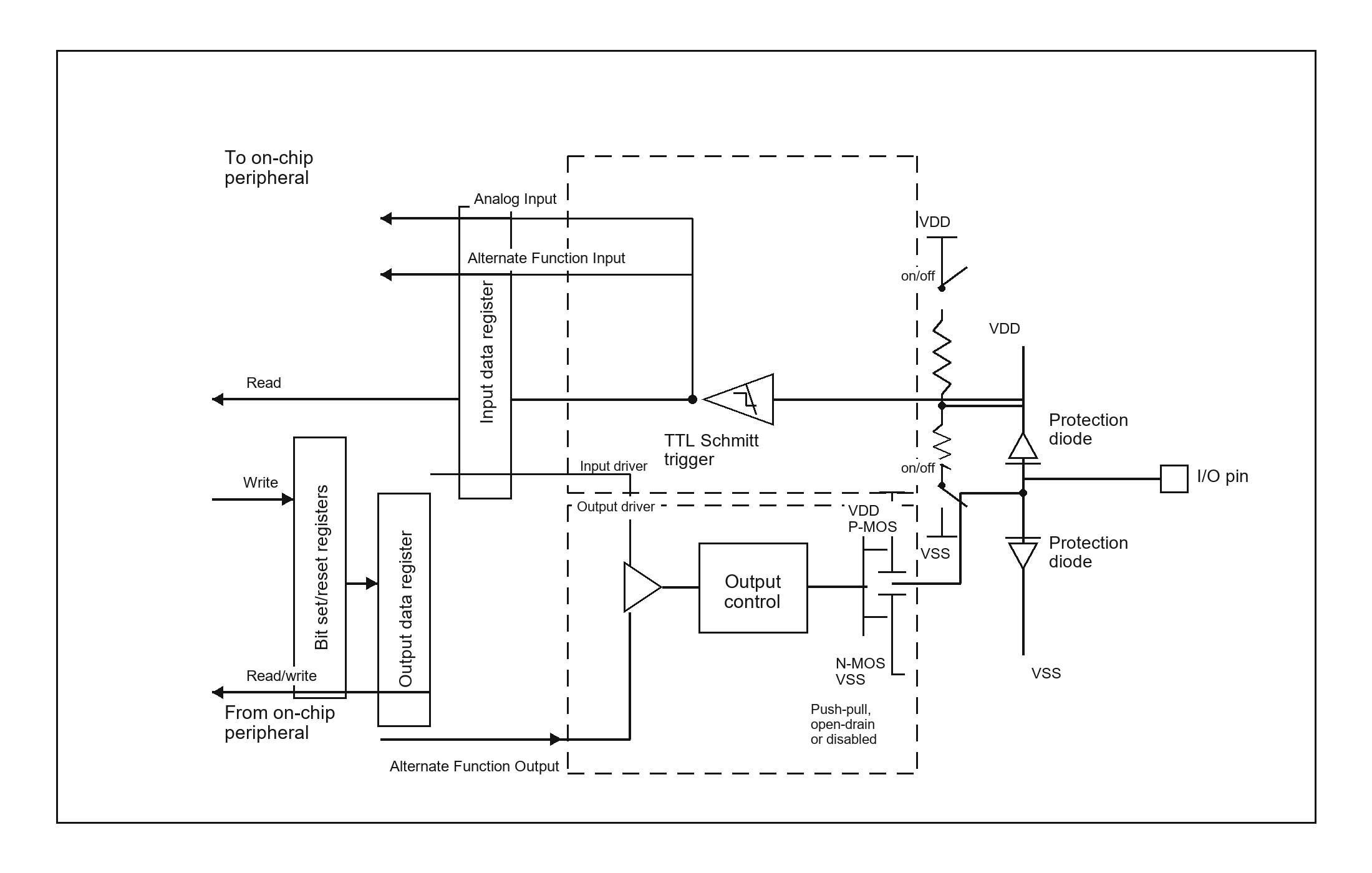
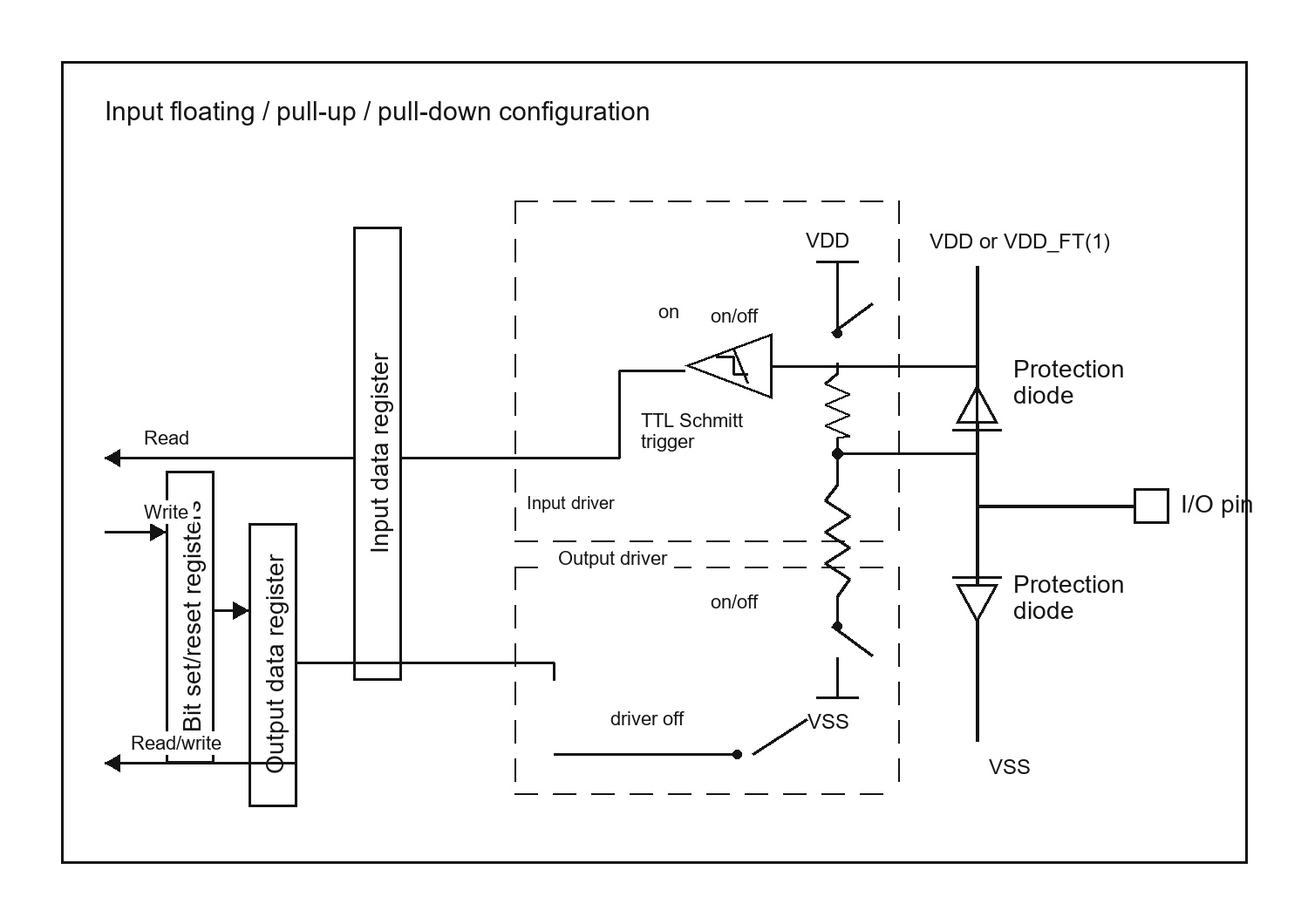
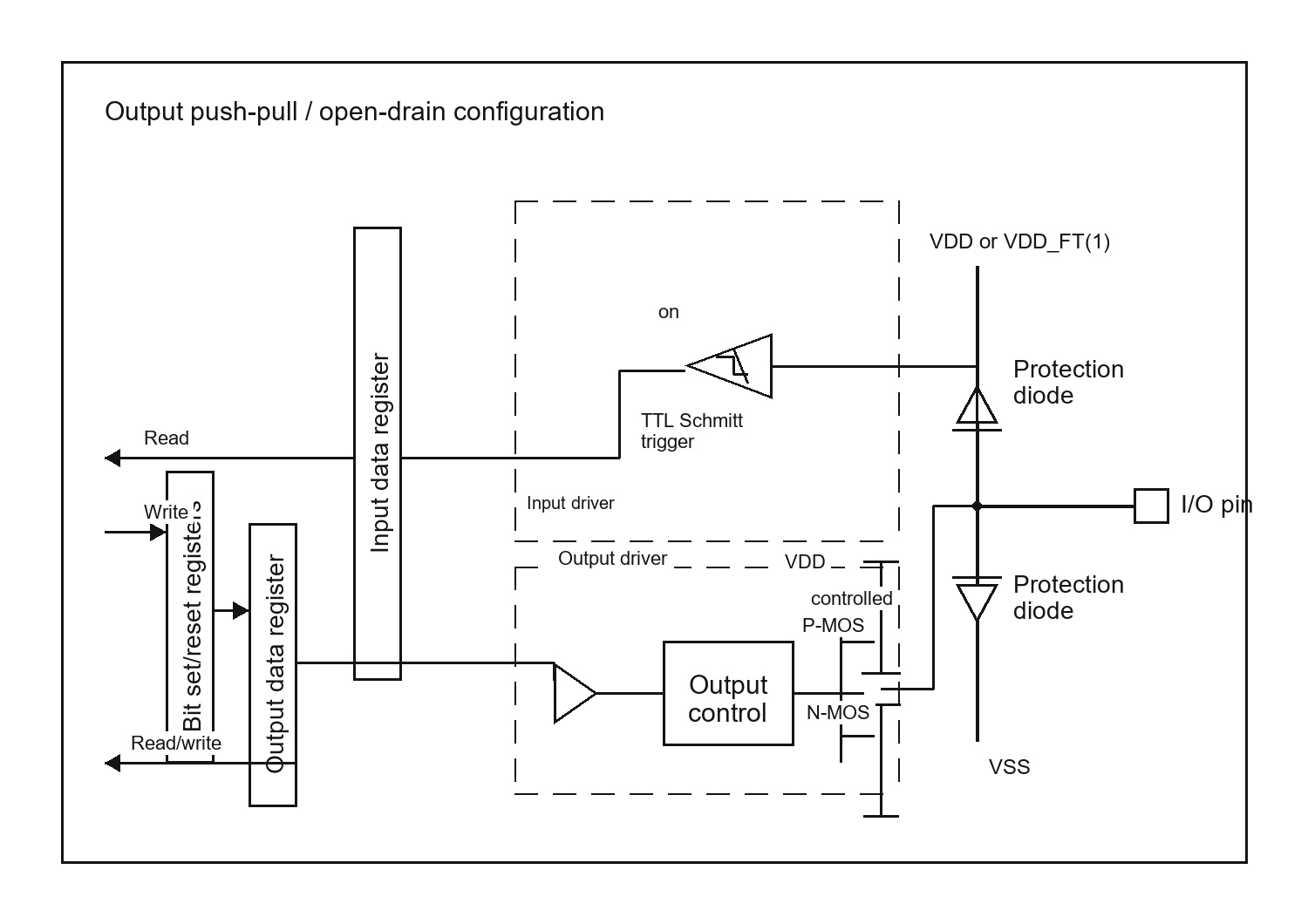
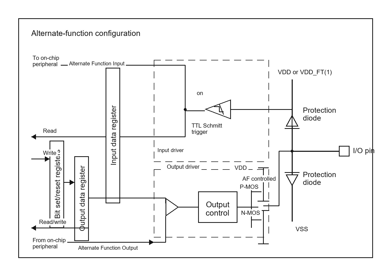
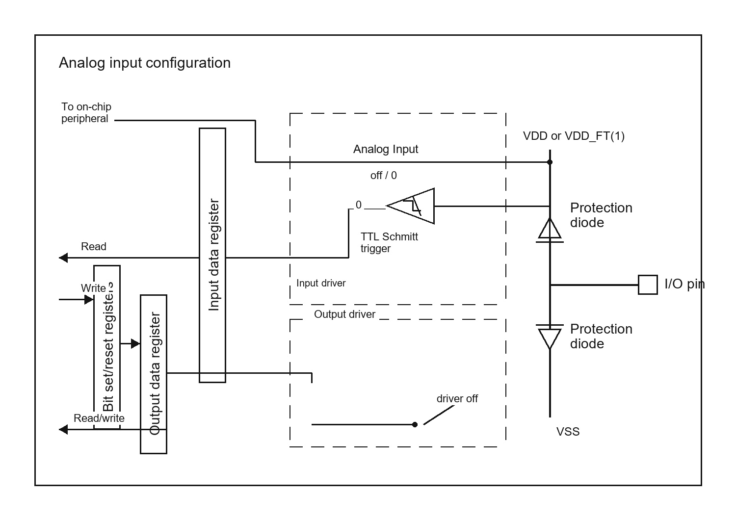
GPIO figures show the input buffer, output driver, alternate-function path, and analog high-impedance path; they are not trainer-board wiring diagrams.
3.1 How to read Figures 2-5
| Figure concept | What it proves | Register path to look for |
|---|
| Input path | IDR reads as 0 on real STM32 behavior when the external pad is low. In the local board route, IDR5 means PA5 / FAULT_IN. | GPIOA_IDR |
| Output path | ODR3 means the PA3 output latch; BS3 sets PA3 / DRV_EN high and BR3 in GPIOA_BSRR resets it low. | GPIOA_ODR, GPIOA_BSRR; GPIOA_BRR is reset-only |
| Analog path | For PA1 / CURRENT_SENSE, PB0 / TEMPERATURE_SENSE, and selectable PA6 / POSITION_IN, GPIO analog mode is only the pad-side prerequisite; ADC channel selection and conversion remain in ADC1. | GPIOA_CRL[7:4], GPIOB_CRL[3:0], GPIOA_CRL[27:24] |
4 I/O port bit configuration
Each pin field is [CNF1 CNF0 MODE1 MODE0]. Section 4.1 tells where the 4-bit field sits inside CRL/CRH; Section 4.2 decodes the value written there into actual STM32F103 pin behavior. The complete configuration truth appears once in Section 4.2.
4.1 Register field placement and pin-number lookup
Read a pin name as Pxy: x selects the port register block and y is the pin number. Thus PA0 uses GPIOA fields with suffix 0, while PB3 uses GPIOB fields with suffix 3. RM0008 defines x=A..G; the current Trainer exposes GPIOA and GPIOB.
| Purpose | Pin range | Field for Pxy | Bit position | Examples |
|---|
| Configure CNF/MODE | y=0..7 | GPIOx_CRL.CNFy/MODEy | nibble [4y+3:4y]
CNFy [4y+3:4y+2]
MODEy [4y+1:4y] | Px0 -> CRL[3:0]
Px3 -> CRL[15:12]
Px7 -> CRL[31:28] |
| Configure CNF/MODE | y=8..15 | GPIOx_CRH.CNFy/MODEy | nibble [4(y-8)+3:4(y-8)]
CNFy [4(y-8)+3:4(y-8)+2]
MODEy [4(y-8)+1:4(y-8)] | Px8 -> CRH[3:0]
Px10 -> CRH[11:8]
Px15 -> CRH[31:28] |
| Read pin input | y=0..15 | GPIOx_IDR.IDRy | IDRy[y] | Px0 -> IDR0[0]
Px15 -> IDR15[15] |
| Store output value | y=0..15 | GPIOx_ODR.ODRy | ODRy[y] | Px0 -> ODR0[0]
Px15 -> ODR15[15] |
| Set output atomically | y=0..15 | GPIOx_BSRR.BSy | BSy[y] | Px0 -> BS0[0]
Px3 -> BS3[3] |
| Reset output through BSRR | y=0..15 | GPIOx_BSRR.BRy | BRy[y+16] | Px0 -> BR0[16]
Px3 -> BR3[19] |
| Reset output through BRR | y=0..15 | GPIOx_BRR.BRy | BRy[y] | Px0 -> BR0[0]
Px3 -> BR3[3] |
| Select configuration lock | y=0..15 | GPIOx_LCKR.LCKy | LCKy[y] | Px0 -> LCK0[0]
Px15 -> LCK15[15] |
Worked lookups: PA0 mode is GPIOA_CRL[3:0], split into CNF0[3:2] and MODE0[1:0]. Its input/output data bit is bit 0; its BSRR set bit is 0, BSRR reset bit is 16, and BRR reset bit is 0. For PA3, x=A, y=3 -> GPIOA_CRL[15:12].
To program a mode without changing neighboring pins, first choose shift = 4*y for CRL or shift = 4*(y-8) for CRH, clear only 0xF << shift, then insert the Section 4.2 nibble at that shift. For example, 0x2 means CNF=00, MODE=10: general-purpose push-pull output, maximum 2 MHz.
4.2 Combined 4-bit nibble value to actual pin behavior
| Nibble | CNF | MODE | Actual STM32F103 pin behavior | Important result |
|---|
| 0x0 (0000) | 00 | 00 | Analog input | Digital input buffer and output driver are disabled. |
| 0x1 (0001) | 00 | 01 | General-purpose push-pull output, max 10 MHz | Output latch drives the pin. |
| 0x2 (0010) | 00 | 10 | General-purpose push-pull output, max 2 MHz | Common control-output setting. |
| 0x3 (0011) | 00 | 11 | General-purpose push-pull output, max 50 MHz | Fastest GPIO output setting. |
| 0x4 (0100) | 01 | 00 | Floating digital input | Reset-state input. |
| 0x5 (0101) | 01 | 01 | General-purpose open-drain output, max 10 MHz | High level requires pull-up. |
| 0x6 (0110) | 01 | 10 | General-purpose open-drain output, max 2 MHz | High level requires pull-up. |
| 0x7 (0111) | 01 | 11 | General-purpose open-drain output, max 50 MHz | High level requires pull-up. |
| 0x8 (1000) | 10 | 00 | Digital input with pull-up / pull-down | ODRy=0 selects pull-down; ODRy=1 selects pull-up. ODR selects the resistor direction here; it does not enable the output driver. |
| 0x9 (1001) | 10 | 01 | Alternate-function push-pull output, max 10 MHz | Peripheral owns output path. |
| 0xA (1010) | 10 | 10 | Alternate-function push-pull output, max 2 MHz | Valid timer/USART AF output. |
| 0xB (1011) | 10 | 11 | Alternate-function push-pull output, max 50 MHz | Used by PA9 USART1_TX and high-speed AF examples. |
| 0xC (1100) | 11 | 00 | Reserved input configuration | Do not use this value. |
| 0xD (1101) | 11 | 01 | Alternate-function open-drain output, max 10 MHz | High level requires pull-up. |
| 0xE (1110) | 11 | 10 | Alternate-function open-drain output, max 2 MHz | High level requires pull-up. |
| 0xF (1111) | 11 | 11 | Alternate-function open-drain output, max 50 MHz | High level requires pull-up. |
STM32F1 naming and MODE pitfall: STM32F103 combines direction, output type, pull selection, and output-speed selection in each CRL/CRH CNFy:MODEy nibble. It does not use the later-family GPIOx_MODER, OTYPER, OSPEEDR, or PUPDR registers. When MODE=00, CNF selects the input type. When MODE!=00, MODE is the maximum GPIO output slew/speed setting—not a timer or PWM frequency—and CNF selects push-pull, open-drain, or alternate-function output.
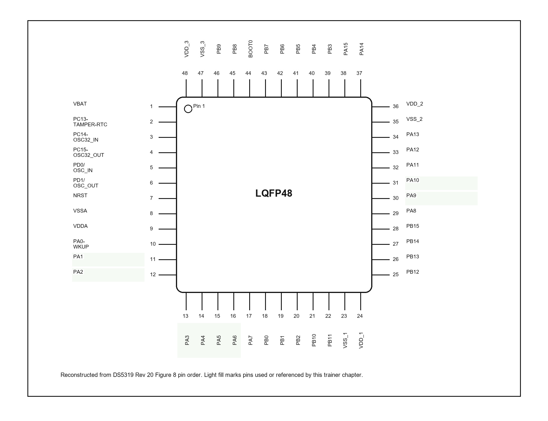
5 Package pinout and pin definitions
5.1 Datasheet-style pin definition excerpt
| Pin | I/O level | Official functions | Locally documented function / route | Register inference / owning chapter / current result |
|---|
| PA1 | I/O | ADC1_IN1 | PA1 / ADC1_IN1 / CURRENT_SENSE | PA1 -> GPIOA_CRL[7:4]; the local board directly samples a 0.05 Ω low-side shunt. This raw path needs Kelvin routing, adequate I²R rating, ADC RC/clamp protection, and a guaranteed 0..VDDA input on real hardware. |
| PA2 | I/O | TIM2_CH3 | PA2 / PWM_OUT trainer route | PA2 -> GPIOA_CRL[11:8]; PA2 is the 0/3.3 V MCU logic PWM command. Trainer proof uses TIM2_CR1.CEN, TIM2_CCER[0], and TIM2_CCR1. Motor A/B are separate VM=12 V H-bridge power terminals. Official pin truth is TIM2_CH3. |
| PA3 | I/O | GPIO output-capable pad | PA3 / DRV_EN | PA3 -> GPIOA_CRL[15:12]; output data path is GPIOA_ODR/BSRR, with GPIOA_BRR as a reset-only alternative. |
| PA5 | I/O | GPIO input-capable pad | PA5 / FAULT_IN | PA5 -> GPIOA_CRL[23:20]; GPIOA_IDR bit 5 is the board-conditioned active-high 3.3 V input. Current fault classes enter through manual Trainer injection; vendor automatic protection thresholds/recovery are reference-only. |
| PA6 | I/O | SPI1_MISO / ADC12_IN6 / TIM3_CH1 / TIM1_BKIN; GPIO input can also source EXTI6 | FEEDBACK_IN: HALL_IN / EXTI6 또는 POSITION_IN / ADC1_IN6 | PA6 -> GPIOA_CRL[27:24]. HALL은 3.3 V 외부 pull-up의 open-collector 디지털 입력이며 AFIO_EXTICR2.EXTI6=0000을 사용합니다. POSITION은 3.3 V AS5600 OUTS=00 / MANG=180° analog input입니다. |
| PA9 | I/O | USART1_TX | Official USART TX route | PA9 -> GPIOA_CRH[7:4]; USART behavior belongs to the USART1 chapter. Current trainer writes to USART1_DR as a TX log effect and has no separate PA9 board wire. |
| PA10 | I/O | USART1_RX | UART_RX | PA10 -> GPIOA_CRH[11:8]; independent External UART TX frames update USART1_SR.RXNE / USART1_DR through the retained UART input route. This input is separate from 3.3 V MCU outputs and the PB0 NTC divider. |
| PB0 | I/O | GPIOB / ADC1_IN8 capable pad | TEMPERATURE_SENSE | GPIOB_CRL[3:0] = 0x0; this is the node between R1 10 kΩ and NTCLE100E3103. The divider is 3.3 V → R1 → PB0 → NTC → GND and is independent of PA10 UART. |
| PB1 | I/O | GPIOB / ADC1_IN9 capable pad | Reference-only | GPIOB_CRL[7:4]; no active System Trainer harness terminal. |
6 Register map and reset values
The port letter selects the base address; every port then uses the same register offsets shown below.
| Port name | Official base address | APB2 clock enable | Current trainer scope |
|---|
| PAy -> GPIOA | 0x40010800 | RCC_APB2ENR.IOPAEN | Register block and current PA routes are exposed. |
| PBy -> GPIOB | 0x40010C00 | RCC_APB2ENR.IOPBEN | GPIOB is exposed; PB0 is the active NTC ADC route and PB1 remains reference-only. |
| Offset | Register | Reset value | Description | Current trainer support |
|---|
| 0x00 | GPIOA_CRL | 0x44444444 | Port configuration register low | Supported through CRL fields. |
| 0x04 | GPIOA_CRH | 0x44444444 | Port configuration register high | Stored and header-accessible. |
| 0x08 | GPIOA_IDR | 0x0000XXXX | Port input data register | Official reset value: 0x0000XXXX; the trainer deliberately starts from 0x00000000, then board-driven input paths update PA5/PA6. |
| 0x0C | GPIOA_ODR | 0x00000000 | Port output data register | Output writes latch only until clock and mode are valid. |
| 0x10 | GPIOA_BSRR | 0x00000000 | Port bit set/reset register | Write side effects update ODR latch bits. |
| 0x14 | GPIOA_BRR | 0x00000000 | Port bit reset register | Reset-only alternative to the BSRR upper BR bits; write side effects clear ODR latch bits. |
| 0x18 | GPIOA_LCKR | 0x00000000 | Port configuration lock register | Stored; lock sequence side effect is not modeled. |
The offset table uses GPIOA names for concrete addresses. Replace GPIOA with GPIOB to address the same fields in the GPIOB block.
7 Register descriptions
For GPIOA_CRL and GPIOA_CRH, use Section 4.1 to locate each 4-bit field and Section 4.2 to decode the written nibble. Current trainer routes and their visible board results remain in Section 8.6.
7.1 Port configuration low register (GPIOA_CRL)
Address offset: 0x00
Reset value: 0x44444444
| Field | Bits | Access / values | Meaning | Current trainer register-value behavior |
|---|
| CNFy[1:0] | 4y+3:4y+2, y=0..7 | rw; interpreted with MODEy | CRL pin configuration bits; decode the combined CNFy/MODEy nibble with Section 4.2. | Changes the trainer interpretation of PA1..PA7 nibbles when the matching clock and route are active. |
| MODEy[1:0] | 4y+1:4y, y=0..7 | rw; 00 = input, 01 = 10 MHz, 10 = 2 MHz, 11 = 50 MHz | CRL input/output and speed bits; their actual pin behavior depends on the paired CNFy value in Section 4.2. | CRL field placement and safe update are modeled for current PA1..PA6 routes. |
7.2 Port configuration high register (GPIOA_CRH)
Address offset: 0x04
Reset value: 0x44444444
| Field | Bits | Access / values | Meaning | Current trainer register-value behavior |
|---|
| CNFy[1:0] | 4(y-8)+3:4(y-8)+2, y=8..15 | rw; interpreted with MODEy | CRH pin configuration bits; decode the combined CNFy/MODEy nibble with Section 4.2. CRH field placement and safe update use 4 * (y - 8). | Stored for PA8..PA15. The current trainer does not drive a separate CRH-controlled GPIO output route. |
| MODEy[1:0] | 4(y-8)+1:4(y-8), y=8..15 | rw; 00 = input, 01 = 10 MHz, 10 = 2 MHz, 11 = 50 MHz | CRH input/output and speed bits; their actual pin behavior depends on the paired CNFy value in Section 4.2. | Stored for official PA9/PA10 USART pin setup; USART behavior is modeled by USART registers, not by CRH pin-mode enforcement. |
7.3 Port input data register (GPIOA_IDR)
Address offset: 0x08
Reset value: 0x0000XXXX
Official reset value: 0x0000XXXX. The trainer deliberately starts from 0x00000000, then board-driven PA5/PA6 inputs update the modeled value.
| Field | Bits | Access / values | Meaning | Current trainer register-value behavior |
|---|
| IDRy | y, y=0..15 | ro | IDRy[y] is the input data bit for pin y. | PA5/PA6 board-driven active-high input values update the modeled IDR; output mode on those routes leaves the board input authoritative. |
7.4 Port output data register (GPIOA_ODR)
Address offset: 0x0C
Reset value: 0x00000000
| Field | Bits | Access / values | Meaning | Current trainer register-value behavior |
|---|
| ODRy | y, y=0..15 | rw | ODRy[y] is the output data latch for pin y. In input pull-up/pull-down mode, this same bit selects the pull direction instead of driving the pad. | For PA3/PA4, the stored latch drives the visible route only when GPIOA clock and output mode are valid; otherwise the UI can report GPIOA clock gated / 0.00 V or Pin mode is not output / 0.00 V. |
7.5 Port bit set/reset register (GPIOA_BSRR)
Address offset: 0x10
Reset value: 0x00000000
| Field | Bits | Access / values | Meaning | Current trainer register-value behavior |
|---|
| BRy | y+16, y=0..15 | w; 0 = no effect, 1 = reset ODRy | BRy[y+16] clears the corresponding output latch. If BSy and BRy are both 1 for one pin in the same write, set has priority. | Writing 1 clears the corresponding trainer ODRy latch; the same-write set-priority rule is modeled. |
| BSy | y, y=0..15 | w; 0 = no effect, 1 = set ODRy | BSy[y] sets the corresponding output latch. | Writing 1 sets the corresponding trainer ODRy latch. |
7.6 Port bit reset register (GPIOA_BRR, reset-only alternative)
Address offset: 0x14
Reset value: 0x00000000
| Field | Bits | Access / values | Meaning | Current trainer register-value behavior |
|---|
| BRy | y, y=0..15 | w; 1 = reset ODRy, 0 = no effect | BRy[y] clears the corresponding output latch. | Writing 1 clears the corresponding trainer ODRy latch. |
7.7 Port configuration lock register (GPIOA_LCKR)
Address offset: 0x18
Reset value: 0x00000000
| Field | Bits | Access / values | Meaning | Current trainer register-value behavior |
|---|
| LCKy | y, y=0..15 | rw | LCKy[y] selects pin y's CRL/CRH configuration for the hardware lock sequence. | Stored; no hard write lock is enforced. |
| LCKK | 16 | rw/read sequence bit | Lock-key bit used by the hardware lock sequence. | LCKK writes are stored; the lock-key sequence is not modeled, so CRL/CRH remain writable in the trainer. |
8 Student register guide and code examples
8.1 Quick first practice path
| Practice | Register action | Site check | Result |
|---|
| Visible GPIO output | Enable clock, set mode nibble, write ODR/BSRR/BRR. | Registers, Board Lab pin routes, Graph, Code Watch, Docs / Log. | Clock + mode + data all matter before voltage appears. |
| Board-driven input | Read GPIOA_IDR for PA5/PA6. | Board Lab pin routes and Registers. | Board-driven input paths update the register. |
8.2 Input configuration sequence
Set MODEy = 00; use 0x4 for floating input or 0x8 for pull-up/down. PA5 is the local GPIO input route PA5 / FAULT_IN.
8.3 Output configuration sequence
Enable IOPAEN, write GPIOA_CRL[15:12] for PA3, then write ODR3, BS3, or BR3. If the setup is wrong, the trainer may show output writes latch only, GPIOA clock gated / 0.00 V, or Pin mode is not output / 0.00 V.
8.4 Practical notes
The current System Trainer named routes are PA10 / UART_RX, PB0 / TEMPERATURE_SENSE, PA1 / CURRENT_SENSE, PA2 / PWM_OUT, PA3 / DRV_EN, PA4 / DRV_DIR, PA5 / FAULT_IN, and selectable PA6 / FEEDBACK_IN.
- Alternate-function outputs still require a correct GPIO nibble and peripheral clock.
- PB0 NTC ADC and PA10 UART are electrically and logically independent inputs.
- HALL uses a 3.3 V open-collector pull-up and executable AFIO_EXTICR2.EXTI6=0000; ANGLE uses AS5600 analog OUT with the local OUTS=00 / MANG=180° profile.
- Vendor sensor tolerances, AS5600 programming/diagnostics, and automatic motor-driver protections are reference-only unless a specific Trainer proof is listed.
8.5 Current trainer code examples
These examples keep the System Trainer mode map and use GPIOA_ODR only for PA3/PA4 output changes.
RCC_APB2ENR opens the port register path, GPIOx_CRL selects each four-bit pin mode,
and ODR bits 3 and 4 directly control the modeled Enable and Direction latches. BSRR/BRR remain part of the official register reference above but are intentionally excluded from this minimum executable path.
As official electrical reference truth, PB1 open-drain drives LOW when ODR1=0 and is released when ODR1=1; PB1 is reference-only and is not part of the executable System harness.
| Example |
Datasheet register path |
Trainer proof to watch |
| GPIOA ODR minimum output check |
IOPAEN, selectable GPIOA_CRL PA6 nibble, and direct GPIOA_ODR bit 3/4 read-modify-write. |
DRV_EN, DRV_DIR, GPIOA_ODR, and Code Watch values. |
GPIOA ODR minimum example: configures the common PA1~PA6 routes and changes only PA3 Enable and PA4 Direction through ODR.
volatile uint32_t gpio_stage = 0u;

void user_init(void)
{
    trainer_clock_init_72mhz();
    RCC->APB2ENR = RCC_APB2ENR_AFIOEN | RCC_APB2ENR_IOPAEN | RCC_APB2ENR_IOPBEN | RCC_APB2ENR_ADC1EN | RCC_APB2ENR_USART1EN;
    RCC->APB1ENR = RCC_APB1ENR_TIM2EN;
    GPIOA->CRL = 0x44422B00u;
    GPIOB->CRL &= ~0xFu; /* PB0 / ADC1_IN8 NTC divider node */
    if (TRAINER->FEEDBACK_MODE == TRAINER_FEEDBACK_ANGLE) {
        GPIOA->CRL &= ~(0xFu << 24);
    } else {
        AFIO->EXTICR[1] &= ~(0xFu << 8); /* EXTI6 = Port A / PA6 */
    }
    GPIOA->ODR &= ~(GPIOA_DRV_EN_BIT | GPIOA_DRV_DIR_BIT);

    watch_u32("gpio_stage", gpio_stage);
    watch_u32("GPIOA_CRL", GPIOA->CRL);
    watch_u32("GPIOA_ODR", GPIOA->ODR);
}

void user_loop(void)
{
    switch (gpio_stage)
    {
        case 0:
            GPIOA->ODR |= GPIOA_DRV_EN_BIT;
            break;
        case 1:
            GPIOA->ODR |= GPIOA_DRV_DIR_BIT;
            break;
        case 2:
            GPIOA->ODR &= ~GPIOA_DRV_EN_BIT;
            break;
        case 3:
            GPIOA->ODR &= ~GPIOA_DRV_DIR_BIT;
            break;
        default:
            break;
    }

    if (gpio_stage < 4u) gpio_stage++;
    watch_u32("gpio_stage", gpio_stage);
    watch_u32("GPIOA_ODR", GPIOA->ODR);
}
8.6 Current System Trainer GPIO connection map
Read each GPIO route in this order: pin-definition evidence first, then the RCC gate, then the GPIO configuration field,
then the data register, then the visible board or UI signal. A pin is GPIO-capable in the STM32-style document when its
package row is an I/O pad and its main reset function is the same port name, such as
PA3 or active NTC input PB0.
PB0 is the active NTC ADC route; PB1 remains only to separate official package truth from the current 8-pin System harness.
| Pin or route |
Datasheet I/O type |
Official GPIO use |
Representative alternate functions |
Currently simulated |
Trainer code result |
| PA0 |
I/O |
GPIO-capable pad on the STM32F103 package row. |
TIM2_CH1_ETR |
No rendered PA0 board node in the current trainer; reference-only for this lab. |
GPIO writes latch in the register model only. |
| PA1 / CURRENT_SENSE |
I/O |
GPIO-capable pad; analog mode is selected for ADC use. |
ADC1_IN1 |
PA1 / ADC1_IN1 / CURRENT_SENSE |
CURRENT_SENSE remains ADC-gated; GPIO output writes latch only. |
| PA3 / PA4 |
I/O |
GPIO output-capable pads. |
General-purpose GPIO routes in this local excerpt. |
DRV_EN and DRV_DIR |
Visible Board Lab pin routes output when IOPAEN, output mode, and data bit writes are present. |
| PA5 / PA6 |
I/O |
GPIO input-capable pads. |
PA6 can feed EXTI6. |
FAULT_IN and HALL_IN / EXTI6 |
Board-driven input paths update GPIOA_IDR; output-mode writes latch only and do not drive FAULT_IN or HALL_IN. PA6 can raise the modeled Hall interrupt. |
| PB0 / TEMPERATURE_SENSE and PB1 official GPIOB reference |
I/O |
GPIO output-capable pads on port B. |
General-purpose GPIOB register behavior in this local excerpt. |
PB0 is ADC1_IN8 / TEMPERATURE_SENSE; PB1 has no active System signal. |
PB0 analog mode and ADC conversion are executable and visible; PB1 remains reference-only. |
| Trainer signal |
Pin-definition evidence |
RCC gate |
GPIO mode field |
Data register path |
Connected board/UI result |
| PA3 / DRV_EN |
PA3 row: Type = I/O, reset function PA3, local route GPIO output. |
RCC->APB2ENR.IOPAEN, bit 2, mask 0x00000004. |
GPIOA_CRL[15:12]; output test uses nibble 0x2: CNF3 = 00, MODE3 = 10, general-purpose push-pull output at 2 MHz. |
GPIOA_ODR bit 3 or GPIOA_BSRR BS3/BR3; GPIOA_BRR bit 3 is reset-only. |
Board Lab pin routes: DRV_EN; feeds the motor-driver enable input. |
| PA4 / DRV_DIR |
PA4 row: Type = I/O, reset function PA4, local route GPIO output. |
RCC->APB2ENR.IOPAEN, bit 2, mask 0x00000004. |
PA4 -> GPIOA_CRL[19:16]; output test uses nibble 0x2: CNF4 = 00, MODE4 = 10, general-purpose push-pull output at 2 MHz. |
GPIOA_ODR bit 4 or GPIOA_BSRR BS4/BR4; GPIOA_BRR bit 4 is reset-only. |
Board Lab pin routes: DRV_DIR; feeds the motor-driver direction input. |
| PA5 / FAULT_IN |
PA5 row: Type = I/O, reset function PA5, local route GPIO input. |
RCC->APB2ENR.IOPAEN, bit 2, mask 0x00000004. |
GPIOA_CRL[23:20]; input test uses nibble 0x4: CNF5 = 01, MODE5 = 00, floating digital input. |
GPIOA_IDR bit 5. |
Board Lab pin routes: FAULT_IN; board-conditioned active-high driver fault input. Selecting output mode in GPIOA_CRL leaves this as a board-driven input route; GPIO writes latch only. |
PA6 / FEEDBACK_IN
HALL / EXTI6 또는 ANGLE / ADC1_IN6 |
Official pin row: Type = I/O, reset function PA6, alternate functions include ADC12_IN6. |
RCC->APB2ENR.AFIOEN bit 0 plus IOPAEN bit 2. |
GPIOA_CRL[27:24]; HALL uses nibble 0x4 floating digital input, ANGLE uses 0x0 analog input. |
HALL: AFIO_EXTICR2.EXTI6=0000, GPIOA_IDR bit 6 and EXTI_IMR/RTSR/PR. ANGLE: ADC_SQR3.SQ1=6 and ADC_DR. |
Board selector and common firmware activate exactly one PA6 source. HALL is 3.3 V open-collector with an external pull-up; ANGLE is AS5600 3.3 V analog OUT with OUTS=00/MANG=180°. |
| PB0 / TEMPERATURE_SENSE |
PB0 is an STM32F103 package I/O pad with ADC1_IN8; the current harness wires the R1/NTC divider node here. |
RCC->APB2ENR.IOPBEN, bit 3, mask 0x00000008. |
GPIOB_CRL[3:0] = 0x0: analog input. |
ADC_SQR3.SQ1=8 → SWSTART → EOC → ADC_DR. |
Board PB0/TEMPERATURE_SENSE, NTC temperature System metric, Registers, Graph, and Watch. PA10/UART_RX remains separate. |
| PB1 official reference |
PB1 is an STM32F103 package I/O pad on GPIOB; current trainer does not wire it. |
RCC->APB2ENR.IOPBEN, bit 3, mask 0x00000008. |
GPIOB_CRL[7:4]; output test uses nibble 0x6: CNF1 = 01, MODE1 = 10, general-purpose open-drain output at 2 MHz. |
GPIOB_ODR bit 1 or GPIOB_BSRR BS1/BR1; GPIOB_BRR bit 1 is reset-only. |
Reference-only register behavior; no Board terminal, graph trace, or active System route. |
GPIO peripheral register description
GPIO-DS001 Rev 1.3