STM32F103 RCC Clock Control Reference Chapter
Clock source selection, SYSCLK distribution, prescalers, and enable registers
RCC User Description: clock-tree and trainer register behavior
Contents
Front matter: Document scope.
- RCC overview
- Clock tree overview
- Derived clocks and important exceptions
- RCC register map
- Clock control register (RCC_CR)
- Clock configuration register (RCC_CFGR)
- AHB/APB enable registers
- Programming sequences
- Student register guide and code examples
Document scope
This chapter follows the official STM32F103 document split: the datasheet provides the big clock-tree view, while RM0008 explains the control registers, prescalers, and peripheral enable sequence. Trainer-executable examples are kept separate in Chapter 9.
1 RCC overview
On STM32F103, RCC performs three jobs. First, it decides which oscillator or PLL output becomes SYSCLK. Second, it divides that system clock into the AHB and APB bus clocks. Third, it enables or disables the bus clock that reaches each peripheral register block.
- HSI, HSE, and PLLCLK are SYSCLK candidates.
- SYSCLK feeds the AHB prescaler to produce HCLK.
- HCLK feeds the APB1 and APB2 prescalers to produce PCLK1 and PCLK2.
- Peripheral registers become readable and writable only after the relevant RCC enable bit is active on real hardware.
2 Clock tree overview
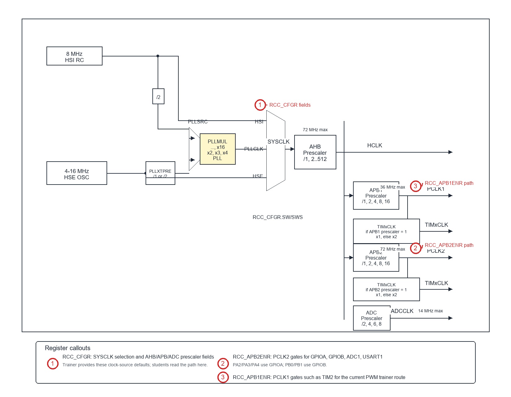
Figure 1. Reconstructed STM32F103 RCC clock-tree slice
Source reconstruction: STM32F103 datasheet (DS5319 Rev 20, Figure 2. Clock tree) and RM0008 Rev 21, Figure 8. Clock tree
The official documents place clock distribution before register details. That order matters because RCC_CR and RCC_CFGR only make sense after the reader can see where SYSCLK, HCLK, PCLK1, PCLK2, and ADCCLK come from.
Figure 1 keeps the clock path uncluttered; exact RCC_CFGR field names and values are listed in Section 6.
- After reset, the internal 8 MHz RC oscillator (HSI) is the default CPU clock.
- AHB and APB2 can run up to 72 MHz.
- APB1 must stay at or below 36 MHz.
- Timer clocks follow the hardware x2 rule whenever the APB prescaler is not 1.
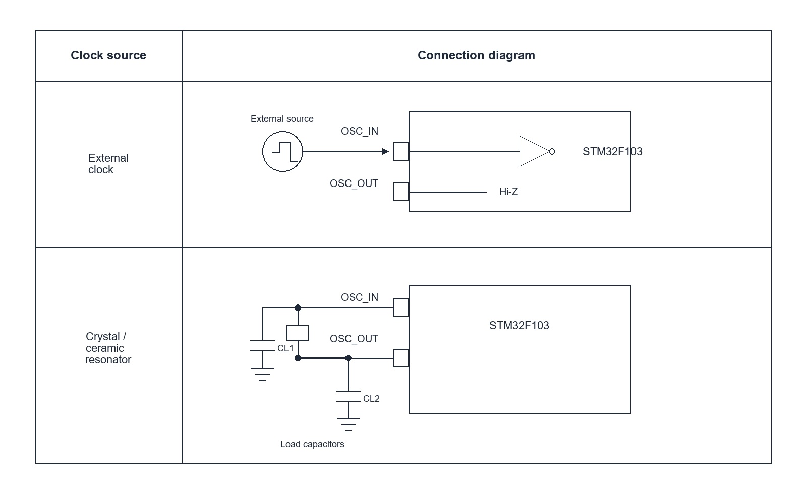
Figure 2. HSE source options: crystal/resonator mode and bypass mode
Source reconstruction: RM0008 Rev 21, Section 7.2.1, Figure 9. HSE/LSE clock sources
3 Derived clocks and important exceptions
| Clock | Generated from | Main consumers | Important limit or rule |
|---|---|---|---|
| SYSCLK | HSI, HSE, or PLLCLK | Core clock root | Selected through RCC_CFGR.SW |
| HCLK | SYSCLK through HPRE | Core, memory, DMA, AHB bus | Maximum 72 MHz |
| PCLK1 | HCLK through PPRE1 | APB1 peripherals such as TIM2, USART2, I2C | Maximum 36 MHz |
| PCLK2 | HCLK through PPRE2 | APB2 peripherals such as GPIO, ADC1, USART1, SPI1, TIM1 | Maximum 72 MHz |
| ADCCLK | PCLK2 through ADCPRE | ADC interface clock | PCLK2 divided by 2, 4, 6, or 8 |
| TIMxCLK | Derived from APB domain clock | TIM1, TIM2, TIM3, TIM4 and similar timers | APB prescaler = 1 then x1, otherwise x2 |
4 RCC register map
This complete low-/medium-/high-density STM32F103 RCC block follows RM0008 Rev 21 Section 7.3.11, Table 18. Absolute addresses use RCC base 0x40021000 + offset; official reset values remain separate from trainer reset and side-effect notes.
| Offset | Absolute address | Register | Official reset | Purpose | Trainer status |
|---|---|---|---|---|---|
| 0x00 | 0x40021000 | RCC_CR | 0x0000XX83 | Clock source enable and ready flags | Header-accessible. Reset starts HSI on/ready; the helper explicitly writes HSE/PLL ready values. Oscillator startup and PLL-lock time are not simulated. |
| 0x04 | 0x40021004 | RCC_CFGR | 0x00000000 | SYSCLK switch, PLL source, PLL multiplier, AHB/APB prescalers, ADC prescaler | Header-accessible. PLL, HCLK, and PCLK1 values affect modeled TIM2 timing; PCLK2 and ADCCLK timing are stored but not modeled. |
| 0x08 | 0x40021008 | RCC_CIR | 0x00000000 | Clock interrupt flags, enables, and clear bits | Stored internally; omitted from the focused Registers list/header, and interrupt/flag-clear side effects are not modeled |
| 0x0C | 0x4002100C | RCC_APB2RSTR | 0x00000000 | APB2 peripheral reset register | Stored internally; omitted from the focused Registers list/header, and peripheral reset side effects are not modeled |
| 0x10 | 0x40021010 | RCC_APB1RSTR | 0x00000000 | APB1 peripheral reset register | Stored internally; omitted from the focused Registers list/header, and peripheral reset side effects are not modeled |
| 0x14 | 0x40021014 | RCC_AHBENR | 0x00000014 | AHB peripheral clock enable register | Stored internally; not exposed as RCC->AHBENR in the focused header or Registers list. AHB gate side effects are not modeled; trainer reset is 0x00000000. |
| 0x18 | 0x40021018 | RCC_APB2ENR | 0x00000000 | APB2 peripheral clock enable register | Header-accessible. AFIO, GPIOA/GPIOB, ADC1, and USART1 gate conditions affect the modeled paths. |
| 0x1C | 0x4002101C | RCC_APB1ENR | 0x00000000 | APB1 peripheral clock enable register | Header-accessible. TIM2EN gates the modeled counter and PWM route. |
| 0x20 | 0x40021020 | RCC_BDCR | 0x00000000 | Backup-domain and RTC clock control register | Stored internally; omitted from the focused Registers list/header, and backup-domain/RTC side effects are not modeled |
| 0x24 | 0x40021024 | RCC_CSR | 0x0C000000 | Low-speed clock control and reset flags | Stored internally; omitted from the focused Registers list/header, low-speed clock/reset-flag side effects are not modeled, and the trainer reset is 0x00000000 |
Official base address: RCC = 0x40021000. Trainer pointer base: RCC = 0x1800. The sandbox block preserves the official offsets above. The focused header exposes CR, CFGR, APB2ENR, and APB1ENR; unsupported positions remain reserved. The sandbox base is not a physical STM32 address.
The three enable registers are expanded separately in Section 7 using the same 32-bit layout and bit-summary format as RCC_CR and RCC_CFGR.
5 Clock control register (RCC_CR)
Address offset: 0x00
Reset value: 0x0000 XX83
| Bit | Name | Access / values | Meaning | Current trainer register-value behavior |
|---|---|---|---|---|
| 0 | HSION | rw; 0 = off, 1 = on | Internal 8 MHz RC enable | Reset value is 1. The bit is stored, but the trainer does not simulate oscillator start/stop timing. |
| 1 | HSIRDY | ro on STM32; reset = 1 | Internal 8 MHz RC ready flag | Reset value is 1. It is not an asynchronously changing trainer signal. |
| 16 | HSEON | rw; 0 = off, 1 = on | External high-speed clock enable | The helper writes 1. A direct write only stores the bit; no crystal startup delay is modeled. |
| 17 | HSERDY | ro on STM32; helper writes 1 | External high-speed clock ready flag | The helper explicitly sets it before its wait loop. The trainer does not raise it automatically after HSEON. |
| 18 | HSEBYP | rw; 0 = crystal, 1 = bypass | External clock bypass | Value is stored for register-layout fidelity; no external clock input model is connected. |
| 24 | PLLON | rw; 0 = off, 1 = on | PLL enable | The helper writes 1. The modeled clock frequency comes from RCC_CFGR, not from a simulated PLL lock process. |
| 25 | PLLRDY | ro on STM32; helper writes 1 | PLL lock flag | The helper explicitly sets it before its wait loop. The trainer does not raise it automatically after PLLON. |
On a device, RCC_CR is the "turn it on and wait until ready" register. In this trainer, the helper preserves that sequence by writing the ready flags itself; do not interpret a raw HSEON or PLLON write as a simulated oscillator or lock event.
6 Clock configuration register (RCC_CFGR)
Address offset: 0x04
Reset value: 0x00000000
| Field / bits | Access / values | Meaning | Current trainer register-value behavior |
|---|---|---|---|
| SW[1:0] | rw; 00 HSI, 01 HSE, 10 PLL | Requested system-clock source | Stored value selects the modeled system clock when SWS is still 00; it therefore changes modeled TIM2 timing. |
| SWS[3:2] | ro on STM32; 00 HSI, 01 HSE, 10 PLL | Reported system-clock source | The helper explicitly writes the status value because the trainer has no automatic hardware handoff. Its stored value takes precedence for modeled TIM2 timing. |
| HPRE[7:4] | rw; /1 to /512 | AHB prescaler from SYSCLK to HCLK | Decoded by the trainer when deriving TIM2 timing. |
| PPRE1[10:8] | rw; /1 to /16 | APB1 prescaler from HCLK to PCLK1 | Decoded by the trainer when deriving TIM2 timing, including the STM32 timer x2 rule when the divider is not /1. |
| PPRE2[13:11] | rw; /1 to /16 | APB2 prescaler from HCLK to PCLK2 | Stored by the helper, but no modeled peripheral timing currently depends on PCLK2. |
| ADCPRE[15:14] | rw; PCLK2 /2, /4, /6, /8 | ADC prescaler | Stored as /6 by the helper; ADC conversion timing is not cycle-accurate in the trainer. |
| PLLSRC[16] | rw; 0 HSI/2, 1 HSE | PLL input source | When the modeled system clock is PLL, this field changes the frequency used for TIM2 timing. |
| PLLXTPRE[17] | rw; 0 HSE, 1 HSE/2 | HSE divider before PLL | When PLLSRC is HSE and PLL is selected, this field changes the frequency used for TIM2 timing. |
| PLLMUL[21:18] | rw; x2 to x16 | PLL multiplication factor | When PLL is selected, the trainer decodes the multiplier for TIM2 timing. The helper uses HSE x9 for 72 MHz. |
RCC_CFGR is the "which clock do I select and how do I divide it" register. The trainer uses its PLL, HCLK, and PCLK1 fields for TIM2 timing, but does not model PCLK2 or ADCCLK timing. SWS is hardware-owned on STM32; the helper writes it explicitly so its status wait loop has a value to read.
7 AHB/APB enable registers
7.1 AHB peripheral clock enable register (RCC_AHBENR)
Address offset: 0x14
Reset value: 0x00000014
| Bit | Name | Access / values | Meaning | Current trainer register-value behavior |
|---|---|---|---|---|
| 0 | DMA1EN | rw; 0 = disabled, 1 = enabled | DMA1 clock enable | Stored internally; not exposed as a focused header/UI field and has no gate side effect. |
| 2 | SRAMEN | rw; 0 = disabled, 1 = enabled | SRAM interface clock enable | Stored internally; not exposed as a focused header/UI field and has no gate side effect. |
| 4 | FLITFEN | rw; 0 = disabled, 1 = enabled | Flash interface clock enable | Stored internally; not exposed as a focused header/UI field and has no gate side effect. |
| 6 | CRCEN | rw; 0 = disabled, 1 = enabled | CRC peripheral clock enable | Stored internally; not exposed as a focused header/UI field and has no gate side effect. |
The official values are stored internally but omitted from the focused Registers list/header because no DMA, SRAM-timing, Flash-interface, or CRC behavior is modeled. GPIO and ADC gates do not belong in this register.
7.2 APB2 peripheral clock enable register (RCC_APB2ENR)
Address offset: 0x18
Reset value: 0x00000000
IOPAEN enables GPIOA for PA2/PA3/PA4, and IOPBEN enables GPIOB for PB0/PB1. Both GPIO port clocks are opened from RCC_APB2ENR; they are not AHB gates.
| Bit | Name | Access / values | Meaning | Current trainer register-value behavior |
|---|---|---|---|---|
| 0 | AFIOEN | rw; 0 = disabled, 1 = enabled | 0x00000001; enables AFIO routing used by the trainer EXTI path | Value 1 opens executable AFIO_EXTICR2; EXTI6=0000 then selects PA6 / HALL_IN. |
| 2 | IOPAEN | rw; 0 = disabled, 1 = enabled | 0x00000004; opens the GPIOA register path | Value 1 gates GPIOA configuration and the modeled PA1-PA6 paths. |
| 3 | IOPBEN | rw; 0 = disabled, 1 = enabled | 0x00000008; opens the official GPIOB register path | Value 1 gates active PB0 / TEMPERATURE_SENSE; PB1 remains reference-only. |
| 9 | ADC1EN | rw; 0 = disabled, 1 = enabled | 0x00000200; opens the ADC1 register path | Value 1 gates PA1 current, PB0 NTC, and selectable PA6 Position conversion. Conversion timing is simplified. |
| 14 | USART1EN | rw; 0 = disabled, 1 = enabled | 0x00004000; opens the trainer USART1 path | Value 1 gates independent PA10 / USART1_RX; this UART input never owns or transports PB0 temperature data. |
| 19 | TIM9EN | rw; 0 = disabled, 1 = enabled | 0x00080000; TIM9 clock-enable field in the RM0008 low/medium/high/XL-density family layout | Reference-only; raw gate bit can latch and remain visible, but no TIM9 behavior is modeled |
| 20 | TIM10EN | rw; 0 = disabled, 1 = enabled | 0x00100000; TIM10 clock-enable field in the RM0008 low/medium/high/XL-density family layout | Reference-only; raw gate bit can latch and remain visible, but no TIM10 behavior is modeled |
| 21 | TIM11EN | rw; 0 = disabled, 1 = enabled | 0x00200000; TIM11 clock-enable field in the RM0008 low/medium/high/XL-density family layout | Reference-only; raw gate bit can latch and remain visible, but no TIM11 behavior is modeled |
RM0008 Rev 21 Section 7.3.7 defines bits 31:22 as reserved, bits 21:19 as TIM11EN/TIM10EN/TIM9EN, and bits 18:16 as reserved. Peripheral availability still depends on the selected STM32F103 device. The trainer has no named TIM9/10/11 header macros, decoded rows, timer blocks, or modeled timer effects. A raw write through RCC->APB2ENR can still latch these bits in MMIO and remain visible in the full APB2ENR hex value. Example supported bit write: RCC->APB2ENR |= (1u << 9);
| Enabled bits | Register value | Use case |
|---|---|---|
| AFIOEN | IOPAEN | 0x00000005 | AFIO + GPIOA |
| AFIOEN | IOPAEN | IOPBEN | 0x0000000D | AFIO + GPIOA + GPIOB |
| AFIOEN | IOPAEN | ADC1EN | 0x00000205 | AFIO + GPIOA + ADC1 |
| AFIOEN | IOPAEN | IOPBEN | ADC1EN | 0x0000020D | AFIO + GPIOA + GPIOB + ADC1 |
Example whole-register write: RCC->APB2ENR = 0x0000020D
7.3 APB1 peripheral clock enable register (RCC_APB1ENR)
Address offset: 0x1C
Reset value: 0x00000000
| Bit | Name | Access / values | Meaning | Current trainer register-value behavior |
|---|---|---|---|---|
| 0 | TIM2EN | rw; 0 = disabled, 1 = enabled | 0x00000001; opens the TIM2 register and trainer PWM path | Value 1 gates the modeled TIM2 counter and PWM route. |
| 1 | TIM3EN | rw; 0 = disabled, 1 = enabled | 0x00000002; TIM3 clock enable on real STM32F103 | Reference-only; value can be stored but no TIM3 block, macro, or UI row is modeled. |
| 17 | USART2EN | rw; 0 = disabled, 1 = enabled | 0x00020000; USART2 clock enable on real STM32F103 | Reference-only; value can be stored but no USART2 block, macro, or UI row is modeled. |
| 21 | I2C1EN | rw; 0 = disabled, 1 = enabled | 0x00200000; I2C1 clock enable on real STM32F103 | Reference-only; value can be stored but no I2C1 block, macro, or UI row is modeled. |
Trainer example: RCC->APB1ENR |= (1u << 0); or RCC->APB1ENR = 0x00000001. A real-device-only TIM2EN | TIM3EN value would be 0x00000003.
8 Programming sequences
Official STM32F103 clock-source switching uses RCC_CR, RCC_CFGR, and FLASH_ACR. The current trainer helper uses the same registers for its fixed 72 MHz profile, then student code opens the modeled APB gates directly.
8.1 Current trainer helper: code-to-register review
This is a review of the executable trainer_clock_init_72mhz() helper, not a replacement for the real-device sequence. This chapter must be enough to analyze the helper code by register value; the companion User Description only adds the learner-facing proof route and exception callouts. RM0008 Rev 21 pages 99-103 define the clock-control fields; pages 111-116 define the AHB/APB enable registers. In particular, HSERDY, PLLRDY, and SWS are hardware-owned status fields on a real STM32F103.
| Helper step | Register value after the helper | Real STM32F103 meaning (RM0008) | Current trainer register-value behavior |
|---|---|---|---|
| FLASH->ACR latency | FLASH_ACR.LATENCY = 2, final 0x00000002 | Two Flash wait states are selected before the 72 MHz clock switch. | When FLASH_ACR.LATENCY=2, the trainer stores the requested Flash-latency value only; it does not add Flash access delay to simulator ticks. |
| HSE enable and ready wait | RCC_CR.HSEON=1, HSERDY=1; final RCC_CR=0x03030083 after all helper steps | HSEON is software-writable. HSERDY is read-only and becomes 1 only when real HSE hardware is stable. | HSEON=1 is stored, but it does not automatically change HSERDY. The helper stores HSERDY=1 to complete its modeled wait loop. |
| PLL source, multiplier, and bus prescalers | PLLSRC=HSE, PLLXTPRE=/1, PLLMUL=×9, HPRE=/1, PPRE1=/2, PPRE2=/1, ADCPRE=/6 | For an 8 MHz HSE source: SYSCLK/HCLK = 72 MHz, PCLK1 = 36 MHz, PCLK2 = 72 MHz, and ADCCLK = 12 MHz. RM0008 limits PCLK1 to 36 MHz. | With PLLSRC=HSE, PLLMUL=×9, HPRE=/1, and PPRE1=/2, the trainer derives the modeled TIM2 clock from the 72 MHz / 36 MHz path. PPRE2 and ADCPRE are stored without a modeled timing side effect. |
| PLL enable and ready wait | RCC_CR.PLLON=1, PLLRDY=1 | PLLON is software-writable. PLLRDY is read-only and is set by hardware only after PLL lock. | PLLON=1 is stored, but it does not automatically change PLLRDY. The helper stores PLLRDY=1 so its modeled wait loop completes; no PLL lock time is simulated. |
| SYSCLK source select and status | RCC_CFGR.SW=PLL, SWS=PLL; final RCC_CFGR=0x001D840A | SW requests the SYSCLK source. SWS is a read-only hardware status field reporting the source actually driving SYSCLK. | SW=PLL requests the PLL source, but the trainer does not automatically mirror SW into SWS. The helper stores SWS=PLL; the clock model then uses that selected-source status when deriving timing. |
| Student peripheral gates | RCC_APB2ENR.IOPAEN=1 and RCC_APB1ENR.TIM2EN=1 in the example | Each enable bit supplies its peripheral clock; it does not configure a GPIO mode, timer period, or output pin. | With IOPAEN=1, modeled GPIOA register-dependent paths are enabled. With TIM2EN=1, the modeled TIM2 counter/PWM path can advance when its own TIM2 and GPIO settings are also valid. |
9 Student register guide and code examples
This final section separates the current trainer code path from the full STM32F103 register path. The main chapter above remains the RCC reference section; this section is the student-oriented bridge into runnable examples.
9.1 Which RCC registers the student should look at
| Register | Current trainer status | Register role | Trainer-visible confirmation |
|---|---|---|---|
| RCC_CR | Header-accessible; used inside trainer_clock_init_72mhz() | Stores HSI/HSE/PLL enable and ready values. The helper writes ready values; oscillator/PLL timing is not simulated. | Add watch_u32("RCC_CR", RCC->CR); this register has no dedicated Registers row. |
| RCC_CFGR | Header-accessible; used inside trainer_clock_init_72mhz() | PLL, HPRE, and PPRE1 values affect modeled TIM2 timing. PPRE2 and ADCPRE are stored but have no timing side effect. | Add watch_u32("RCC_CFGR", RCC->CFGR); this register has no dedicated Registers row. |
| RCC_APB2ENR | Used directly in current trainer examples | Enables the modeled AFIO, GPIOA, GPIOB, ADC1, and USART1 register paths. | Registers -> Clock shows AFIOEN, IOPAEN, IOPBEN, ADC1EN, and USART1EN as ON/OFF rows. |
| RCC_APB1ENR | Used directly in current trainer examples | Enables the modeled TIM2 counter and PWM route. | Registers -> Clock shows TIM2EN as an ON/OFF row. |
| FLASH_ACR | Used inside trainer_clock_init_72mhz() | The helper stores latency 2 before selecting PLL. Flash wait-state delay itself is not simulated. | Add Code Watch when inspecting the value; there is no dedicated Registers row. |
9.2 Current trainer route and enable examples
An RCC enable opens the peripheral clock and register path; RCC does not select or own the 4-bit GPIO nibble. The actual pin behavior is determined by the matching GPIOx_CRL / GPIOx_CRH field and, when applicable, the peripheral chapter linked below.
| Peripheral / route | Required RCC enable | Then configure | Related chapter |
|---|---|---|---|
| GPIOA output or input | GPIOA sits on APB2, so enable RCC->APB2ENR.IOPAEN. | Program GPIOA_CRL / GPIOA_CRH, then use IDR, ODR, BSRR, or BRR. | GPIOA chapter |
| ADC1 reading on PA1 / CURRENT_SENSE | GPIOA and ADC1 both sit on APB2, so enable IOPAEN and ADC1EN. Official STM32 flow also derives ADCCLK from PCLK2 through RCC_CFGR.ADCPRE. | Place PA1 in analog mode, then configure ADC channel selection, sample time, and conversion start logic. | ADC1 chapter |
| ADC1 reading on PB0 / TEMPERATURE_SENSE | Enable IOPBEN and ADC1EN. | Configure PB0 analog mode, then use SQ1=8 → SWSTART → EOC → ADC_DR. PA10 UART remains a separate USART1 route. | ADC1 + GPIOB chapters |
| ADC1 reading on selectable PA6 / POSITION_IN | Enable IOPAEN and ADC1EN. | Configure PA6 analog mode, then use SQ1=6 and SWSTART. AS5600 power/output programming is not an RCC function. | ADC1 + GPIOA chapters |
| TIM2 PWM output on the trainer route | TIM2 sits on APB1, so enable RCC->APB1ENR.TIM2EN. The routed pad still needs its GPIO port clock. | Configure the GPIO pin for alternate-function output and then program timer output enable and duty registers. | TIM2 + GPIOA chapters |
| EXTI6-related routing for PA6 / HALL_IN | AFIO and the GPIO port depend on APB2 clock enables. | Configure the pad mode, write AFIO_EXTICR2.EXTI6=0000 for Port A, then program the interrupt registers. | EXTI and GPIOA chapters |
9.3 Clock-source checkpoint before trainer gates
Before opening APB peripheral gates, read the clock-source path first: HSI/HSE/PLL -> SYSCLK -> HCLK -> PCLK1/PCLK2. RM0008 describes the HSI reset/default path through RCC_CR.HSION, RCC_CR.HSIRDY, RCC_CFGR.SW, and RCC_CFGR.SWS. The current trainer exposes the real initialization sequence as trainer_clock_init_72mhz() in training_api.h, then lets student code open the modeled APB gates it needs. RCC_AHBENR is not part of the focused student header.
| Datasheet / RM0008 item to check first | Official meaning | Current trainer support |
|---|---|---|
| RCC_CR.HSION / RCC_CR.HSIRDY | Turns on the internal 8 MHz HSI oscillator and reports when it is stable. | Reset defaults keep HSI on/ready. The values are stored; the trainer does not simulate HSI startup or automatically change HSIRDY. |
| RCC_CFGR.SW = 00 / RCC_CFGR.SWS = 00 | Selects HSI as SYSCLK and reports that HSI is the active system clock. | Exposed in training_api.h. The helper explicitly writes SWS so its wait loop completes; the trainer does not automatically mirror SW into SWS. |
| FLASH_ACR.LATENCY | Sets Flash wait states before high-frequency SYSCLK operation. | Exposed through FLASH->ACR and configured by trainer_clock_init_72mhz(); its wait-state delay is not simulated. |
| RCC_APB2ENR / RCC_APB1ENR | Opens the peripheral register blocks after the clock tree decision is understood. | Trainer-executable; these final peripheral gates remain direct student code. |
9.4 Current trainer code example
void user_init(void)
{
    // Configure the trainer RCC_CR/RCC_CFGR 72 MHz helper path.
    // HSE 8 MHz -> PLL x9 -> SYSCLK 72 MHz is stored by the helper.
    trainer_clock_init_72mhz();

    // Common gate set: AFIO, GPIOA, GPIOB, ADC1 and independent USART1 on APB2.
    RCC->APB2ENR = RCC_APB2ENR_AFIOEN | RCC_APB2ENR_IOPAEN | RCC_APB2ENR_IOPBEN | RCC_APB2ENR_ADC1EN | RCC_APB2ENR_USART1EN;

    // TIM2 PWM gate on APB1.
    RCC->APB1ENR = RCC_APB1ENR_TIM2EN;
}

void user_loop(void)
{
}
This is the System Trainer common gate set used by RCC, GPIO, ADC, TIM2 PWM, motor-driver, independent PA10 UART, and PB0 NTC examples. GPIOB/PB0 is active for TEMPERATURE_SENSE; PB1 remains reference-only. RCC only opens register paths: NTC divider physics, AS5600 OUTS/MANG programming, Hall pull-up voltage, shunt protection, and driver fault physics are owned by their hardware-interface documents.
9.5 Full STM32F103 register sequence behind the helper
Reference-only on real STM32F103 hardware: use the Section 9.4 helper in the current trainer. This polling sequence expects hardware-owned ready and clock-switch status bits to change while the code is running, so it is not a pasteable trainer replacement for trainer_clock_init_72mhz().
/* Full-register STM32F103 example: HSE 8 MHz -> PLL x9 -> SYSCLK 72 MHz */
FLASH->ACR |= 0x2u;                 /* FLASH latency = 2 before 72 MHz */

RCC->CR |= (1u << 16);             /* HSEON: HSE source ON */
while ((RCC->CR & (1u << 17)) == 0u) { }   /* HSERDY: HSE stable */

{
    uint32_t cfgr = RCC->CFGR;
    cfgr &= ~((1u << 16) | (1u << 17) | (0xFu << 18) | (0xFu << 4) | (0x7u << 8) | (0x7u << 11) | (0x3u << 14));
    cfgr |=
        (1u << 16) |               /* PLLSRC = HSE: HSE -> PLL path */
        (0u << 17) |               /* PLLXTPRE = /1 */
        (7u << 18) |               /* PLLMUL = x9 */
        (0u << 4)  |               /* HPRE = /1 */
        (4u << 8)  |               /* PPRE1 = /2 */
        (0u << 11) |               /* PPRE2 = /1 */
        (2u << 14);                /* ADCPRE = /6 */
    RCC->CFGR = cfgr;
}

RCC->CR |= (1u << 24);             /* PLLON: PLL source ON */
while ((RCC->CR & (1u << 25)) == 0u) { }   /* PLLRDY: PLL stable */

RCC->CFGR = (RCC->CFGR & ~0x3u) | 0x2u;    /* SW = PLL */
while (((RCC->CFGR >> 2) & 0x3u) != 0x2u) { }   /* SWS = PLL */
This example shows the full-device clock-source path using RCC_CR, RCC_CFGR, and FLASH_ACR. Read it along the Figure 1 path: HSE -> PLLXTPRE -> PLL -> SW -> SYSCLK -> AHB/APB/ADC Prescaler. For the HSE 8 MHz -> PLL x9 -> 72 MHz route, PLLSRC = 1 selects HSE as the PLL input. The trainer helper performs the equivalent setup and explicitly writes the ready/status bits because no automatic oscillator or PLL state transition is modeled; use that helper for code that must run inside one user_init() phase.