TIM2 PWM Reference Chapter
STM32F103 TIM2 PWM path, official-layout register block, and trainer route boundary
TIM2/PWM User Description: trainer route and visible behavior
Contents
- Official reference basis
- PWM generation path
- Pin and clock routing
- Register map and simulated subset
- Register descriptions
- Student register guide and code examples
1 Official reference basis
| Source | Relevant item | Use in this chapter |
|---|---|---|
| STM32F103x8/xB datasheet DS5319 Rev 20 | Table 5, alternate functions | Pin truth: PA0 = TIM2_CH1_ETR, PA2 = TIM2_CH3, PA15 can be TIM2_CH1_ETR after remap. |
| STM32F10xxx reference manual RM0008 Rev 21 | RCC section 7.3.8 | RCC->APB1ENR.TIM2EN gates TIM2. |
| RM0008 Rev 21 | Timer section 15, PWM mode and registers | PSC, ARR, CNT, CCMR1.OC1M, CCMR1.OC1PE, CCR1, CCER.CC1E, and CR1.CEN are the real PWM control path. |
| RM0008 Rev 21 | GPIO section 9, alternate function output | Real PWM output requires the GPIO pin configured as alternate-function output, commonly push-pull for this route. |
2 PWM generation path
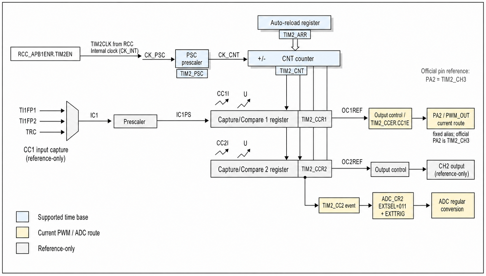
Reconstructed from RM0008 Rev 21 Figure 100, General-purpose timer block diagram, and scoped to the current simulator/runtime contract. The figure keeps the official shared counter/compare structure, representative CC1 input-selection MUX, IC1PS, CC1I/CC2I, and OC1REF/OC2REF signal language. Blue marks the supported time base; yellow marks the current implementation CCR1 -> PWM_OUT and TIM2_CC2 -> ADC routes; grey marks reference-only behavior. The current implementation ADC branch is the modeled TIM2_CC2 event accepted only with ADC_CR2.ADON=1 + EXTSEL=011 + EXTTRIG, not TRGO. The full trigger/slave block and unused channel lanes are intentionally omitted from this principle figure and remain reference-manual concepts.
CC1I/CC2I identify the official capture/compare interrupt or DMA request outputs, and U identifies the update event. They preserve RM0008 signal language for reading the figure, but their request/flag side effects are Reference-only in the current implementation.
This chapter is intentionally TIM2-only. The RM0008 TIM1/TIM8 advanced-control-only repetition counter, dead-time/break, complementary-output, and trigger/slave paths are Reference-only; the current implementation exposes an executable TIM2 focused register/header/UI path.
In official PWM mode 1, the output reference is active while CNT < CCRx and inactive for the rest of the period, subject to polarity and output enable settings. In PWM mode 2, the active/inactive relation is inverted. With an up-counting timer, the counter clock is TIMxCLK / (PSC + 1), the PWM period is approximately (ARR + 1) / counter_clock, and the active-high duty ratio is approximately CCR / (ARR + 1).
The trainer derives TIM2CLK from the modeled RCC clock tree, then advances CNT by elapsed timer cycles after the PSC + 1 division. The PWM period and duty therefore follow TIM2CLK / ((PSC + 1) × (ARR + 1)) and CCR1 / (ARR + 1). Board Lab pin routes renders the average PA2 / PWM_OUT voltage; Graph exposes PWM toggle and average probes, while Log records the derived frequency and period. Figure 1 is the only principle figure: it connects the time base to the trainer's observable CCR1 PWM and CCR2 ADC-trigger routes. On real hardware, preload bits and EGR.UG control shadow-register transfers; those side effects remain reference-only in the trainer. The official pin truth remains: PA2 is TIM2_CH3, while the trainer uses its fixed TIM2_CCR1 route. For a step-by-step ARR/CNT rollover and CNT/CCR1 compare example, continue to the TIM2/PWM User Description learning appendix.
3 Pin and clock routing
| Layer | Official STM32F103 fact | Current trainer contract |
|---|---|---|
| Clock | TIM2 is on APB1, so enable RCC->APB1ENR.TIM2EN. Enable RCC->APB2ENR.IOPAEN to configure the default GPIOA pin path. AFIOEN is needed only when software accesses AFIO registers, such as AFIO_MAPR for a remapped timer pin. | The simulator gates the PWM effect on TIM2EN, IOPAEN, an output-capable PA2 nibble, CC1E, and CEN. It does not require AFIOEN for the fixed PA2 trainer route. |
| GPIO AF | Real output compare pins must be configured through GPIO alternate-function output mode. | GPIOA_CRL PA2 configuration is displayed, but the route is a simplified trainer path. |
| Channel 1 pin | TIM2_CH1 is on PA0 by default and PA15 after remap. | The trainer uses TIM2_CCR1 and TIM2_CCER.CC1E for its fixed PA2 duty/output gate. |
| PA2 pin | PA2 is TIM2_CH3 on the real STM32F103; official PA2 PWM would use TIM2_CCR3. | The board labels this as PA2 / PWM_OUT trainer route. The trainer's TIM2_CCR1 duty field is an alias for this route, not an official PA2 channel-1 mapping. |
3.1 PA2 GPIO nibble before PWM output
| Pin / route | GPIO field | 4-bit value | Actual STM32F103 behavior | Current trainer result |
|---|---|---|---|---|
| PA2 / TIM2_CH3 official / PWM_OUT trainer | GPIOA_CRL[11:8], shift 8, mask 0x00000F00 | 0xB (1011): CNF=10, MODE=11 | Alternate-function push-pull output, max 50 MHz. On the real device PA2 is TIM2_CH3 and therefore uses CCR3; 0xA is the 2 MHz AF push-pull alternative. | The trainer checks only MODE != 00, then uses the fixed CCR1 alias with TIM2EN + CC1E + CEN. The executable example below uses official-style 0xB; compact lab code using 0x2 is accepted only because the trainer simplifies the mux. |
The full GPIO nibble table is in the GPIO Register Datasheet. The PA2 field write is GPIOA->CRL = (GPIOA->CRL & ~(0xFu << 8)) | (0xBu << 8).
4 Register map and simulated subset
| Register | Trainer support | Main role | Read it together with |
|---|---|---|---|
| RCC_APB1ENR | 지원됨 | Turns on the TIM2 register block on APB1. | Figure 1 trainer clock gate and TIM2_CCER. |
| RCC_APB2ENR | 지원됨 | IOPAEN opens GPIOA register access for the default pin path. AFIOEN is separate and is required only before AFIO register access or remapping. | Section 3 pin path and GPIOA_CRL. |
| GPIOA_CRL | 지원됨 | Places PA2 in alternate-function push-pull style for the trainer PWM route. | Section 3 route table and official pin-truth row. |
| TIM2_CR1 | 지원됨 | CEN starts the modeled counter and is required with TIM2EN and CC1E for the trainer PWM route. Other CR1 controls remain official reference behavior. | Figure 1 counter-enable input and User Description. |
| TIM2_PSC / TIM2_ARR / TIM2_CNT | 지원됨 | Define the modeled counter rate, period, and current count. | Figure 1 and Log timing message. |
| TIM2_CCR1 | 지원됨 | Stores the compare count; with ARR = 99, 60 produces 60% duty on the trainer PA2 route. | Figure 1 and Graph PA2 / PWM_OUT toggle. |
| TIM2_CCR2 | 지원됨 | Emits the modeled TIM2_CC2 compare event when CNT crosses CCR2. ADC conversion starts only when the ADC1 clock, PA1 analog mode, SQR3 channel 1, and ADC_CR2.ADON=1 + EXTSEL=011 + EXTTRIG are also configured. | Figure 1 and ADC User Description. |
| TIM2_CCER | 지원됨 | Bit 0, CC1E, opens the trainer PWM output alias when TIM2_CR1.CEN is also set. | Figure 1 and Board Lab pin routes PWM_OUT. |
| TIM2_SR | 미지원 | Official status flags are documented below, but flag generation and write-to-clear side effects are not modeled as student-visible behavior. | Official status behavior and User Description boundary row. |
| TIM2_CCMR1 / TIM2_EGR | 미지원 | Official PWM-mode, preload, and software-event fields are documented below. The current trainer's executable path does not expose these fields in training_api.h or enforce their side effects. | Official RM0008 behavior and User Description boundary rows. |
4.1 Complete official TIM2 register map
RM0008 Rev 21 Table 88 defines the full TIM2-to-TIM5 layout. Absolute addresses below use TIM2 base 0x40000000 + offset. Official reset values stay separate from trainer-specific reset and support notes.
| Offset | Absolute address | Register | Official reset | Trainer status | Description |
|---|---|---|---|---|---|
| 0x00 | 0x40000000 | TIM2_CR1 | 0x00000000 | 지원됨 | CEN starts the modeled counter. |
| 0x04 | 0x40000004 | TIM2_CR2 | 0x00000000 | 미지원 | Master-mode and control-2 fields are not exposed by the focused trainer block. |
| 0x08 | 0x40000008 | TIM2_SMCR | 0x00000000 | 미지원 | Slave-mode, trigger, and external clock controls. |
| 0x0C | 0x4000000C | TIM2_DIER | 0x00000000 | 미지원 | DMA and interrupt enable register. |
| 0x10 | 0x40000010 | TIM2_SR | 0x00000000 | 미지원 | Official update/compare flag generation and write-to-clear side effects are not modeled. Section 5.5 preserves the official flag meanings, but the student UI/header does not expose TIM2_SR. |
| 0x14 | 0x40000014 | TIM2_EGR | 0x00000000 | 미지원 | Write-1 software event generation is not executed. |
| 0x18 | 0x40000018 | TIM2_CCMR1 | 0x00000000 | 미지원 | PWM-mode and preload side effects are not enforced. |
| 0x1C | 0x4000001C | TIM2_CCMR2 | 0x00000000 | 미지원 | Capture/compare mode register for channels 3 and 4. |
| 0x20 | 0x40000020 | TIM2_CCER | 0x00000000 | 지원됨 | CC1E opens the fixed PA2/PWM_OUT trainer route when CEN is set. |
| 0x24 | 0x40000024 | TIM2_CNT | 0x00000000 | 지원됨 | Modeled 16-bit up-counter value. |
| 0x28 | 0x40000028 | TIM2_PSC | 0x00000000 | 지원됨 | Counter clock divisor is PSC + 1. |
| 0x2C | 0x4000002C | TIM2_ARR | 0x0000FFFF | 지원됨 | Period count is ARR + 1; Trainer reset 0x00000063 (99) is used for the focused lesson. |
| 0x30 | 0x40000030 | Reserved | - | - | Reserved address slot in the official TIM2 map. |
| 0x34 | 0x40000034 | TIM2_CCR1 | 0x00000000 | 지원됨 | PWM compare count; duty is CCR1 / (ARR + 1) on the trainer alias. |
| 0x38 | 0x40000038 | TIM2_CCR2 | 0x00000000 | 지원됨 | Compare count for the modeled TIM2_CC2 event. ADC conversion also requires ADC_CR2.ADON=1 and the matching ADC1 trigger configuration. |
| 0x3C | 0x4000003C | TIM2_CCR3 | 0x00000000 | 미지원 | Official channel-3 capture/compare register, including the real PA2 PWM channel. |
| 0x40 | 0x40000040 | TIM2_CCR4 | 0x00000000 | 미지원 | Official channel-4 capture/compare register. |
| 0x44 | 0x40000044 | Reserved | - | - | Reserved address slot in the official TIM2 map. |
| 0x48 | 0x40000048 | TIM2_DCR | 0x00000000 | 미지원 | DMA control register. |
| 0x4C | 0x4000004C | TIM2_DMAR | 0x00000000 | 미지원 | DMA address for full-transfer access. |
5 Register descriptions
Each official TIM2 register now has its own address/reset line, 32-bit field layout, field table, and current Trainer boundary. Registers marked 미지원 remain here for RM0008 navigation and must not be read as executable Trainer features.
5.1 Control register 1 (TIM2_CR1)
Address offset: 0x00 Address: 0x40000000 Reset value: 0x00000000
| Bit | Name | Access / values | Meaning | Current trainer register-value behavior |
|---|---|---|---|---|
| 31:10 | Reserved | - | Keep at reset value. | - |
| 9:8 | CKD[1:0] | rw; 00 = tDTS=tCK_INT, 01 = 2×tCK_INT, 10 = 4×tCK_INT, 11 = Reserved | Clock division ratio used by the digital filters and dead-time sampling clock. | 미지원; the modeled counter clock is divided only by PSC + 1. |
| 7 | ARPE | rw; 0 = ARR not buffered, 1 = ARR buffered | Auto-reload preload enable. | 미지원; stored ARR is used directly. |
| 6:5 | CMS[1:0] | rw; 00 = edge-aligned, 01/10/11 = center-aligned modes 1/2/3 | Counter alignment mode. | 미지원; the Trainer uses an up-counting edge-aligned path. |
| 4 | DIR | rw; 0 = upcounter, 1 = downcounter | Direction in edge-aligned mode. | 미지원; the Trainer counts up. |
| 3 | OPM | rw; 0 = continuous, 1 = stop at next update event | One-pulse mode. | 미지원; CEN is not auto-cleared. |
| 2 | URS | rw; 0 = any documented source, 1 = overflow/underflow only | Selects which sources can generate an update request. | 미지원; update interrupt/DMA request behavior is not modeled. |
| 1 | UDIS | rw; 0 = update event enabled, 1 = update event disabled | Disables update-event generation. | 미지원; shadow-register transfers are not modeled. |
| 0 | CEN | rw; 0 = counter disabled, 1 = counter enabled | Starts or stops the counter; clearing CEN does not clear CNT. | 지원됨; starts and stops the modeled counter. |
5.2 Control register 2 (TIM2_CR2)
Address offset: 0x04 Address: 0x40000004 Reset value: 0x00000000
| Bit | Name | Access / values | Meaning | Current trainer register-value behavior |
|---|---|---|---|---|
| 31:8, 2:0 | Reserved | - | Keep at reset value. | - |
| 7 | TI1S | rw; 0 = TI1 from CH1, 1 = XOR of CH1/CH2/CH3 | Selects the TI1 input source. | 미지원. |
| 6:4 | MMS[2:0] | rw; 000 reset, 001 CEN, 010 update, 011 compare pulse, 100/101/110/111 OC1REF/OC2REF/OC3REF/OC4REF | Selects the signal sent on the timer TRGO master output. | 미지원; the Trainer ADC route uses the fixed TIM2_CC2 event, not TIM2_TRGO. |
| 3 | CCDS | rw; 0 = CCx DMA request on CCx event, 1 = on update event | Selects capture/compare DMA request timing. | 미지원. |
5.3 Slave mode control register (TIM2_SMCR)
Address offset: 0x08 Address: 0x40000008 Reset value: 0x00000000
| Bit | Name | Access / values | Meaning | Current trainer register-value behavior |
|---|---|---|---|---|
| 31:16, 3 | Reserved | - | Keep at reset value. | - |
| 15 | ETP | rw; 0 = non-inverted/high or rising, 1 = inverted/low or falling | External trigger polarity. | 미지원. |
| 14 | ECE | rw; 0 = external clock mode 2 disabled, 1 = enabled | Enables external clock mode 2. | 미지원. |
| 13:12 | ETPS[1:0] | rw; 00 = off, 01 = /2, 10 = /4, 11 = /8 | External trigger prescaler. | 미지원. |
| 11:8 | ETF[3:0] | rw; 0000 = no filter; 0001..1111 select RM0008 sampling-clock/N combinations | Digital filter for the external trigger. Codes progress from fCK_INT, N=2/4/8 through fDTS/32, N=5/6/8. | 미지원. |
| 7 | MSM | rw; 0 = no master/slave synchronization, 1 = synchronized | Delays trigger effects to synchronize timers. | 미지원. |
| 6:4 | TS[2:0] | rw; 000..011 = ITR0..ITR3, 100 = TI1 edge detector, 101 = TI1FP1, 110 = TI2FP2, 111 = ETRF | Selects the trigger input. | 미지원. |
| 2:0 | SMS[2:0] | rw; 000 disabled, 001/010/011 encoder modes 1/2/3, 100 reset, 101 gated, 110 trigger, 111 external clock mode 1 | Selects slave or encoder operating mode. | 미지원; trigger/slave and encoder paths are not modeled. |
5.4 DMA / interrupt enable register (TIM2_DIER)
Address offset: 0x0C Address: 0x4000000C Reset value: 0x00000000
| Bit | Name | Access / values | Meaning | Current trainer register-value behavior |
|---|---|---|---|---|
| 31:15, 13, 7, 5 | Reserved | - | Keep at reset value. | - |
| 14, 12:8 | TDE, CC4DE..CC1DE, UDE | rw; each bit 0 = DMA request disabled, 1 = enabled | Enables trigger, capture/compare, and update DMA requests. | 미지원; TIM2 DMA requests are not modeled. |
| 6, 4:0 | TIE, CC4IE..CC1IE, UIE | rw; each bit 0 = interrupt disabled, 1 = enabled | Enables trigger, capture/compare, and update interrupt requests. | 미지원; TIM2 interrupt requests are not modeled. |
5.5 Status register (TIM2_SR)
Address offset: 0x10 Address: 0x40000010 Reset value: 0x00000000
| Bit | Name | Access / values | Meaning | Current trainer register-value behavior |
|---|---|---|---|---|
| 31:13, 8:7, 5 | Reserved | - | Keep at reset value. | - |
| 12:9 | CC4OF..CC1OF | rc_w0; 0 = no overcapture, 1 = overcapture detected | Input-capture overcapture flags. | 미지원; flags and write-to-clear effects are not exposed. |
| 6 | TIF | rc_w0; 0 = no trigger event, 1 = trigger event pending | Trigger interrupt flag. | 미지원. |
| 4:1 | CC4IF..CC1IF | rc_w0; 0 = no event pending, 1 = capture/compare event pending | Set by the corresponding capture event or output-compare match, according to channel mode. | 미지원; the Trainer logs TIM2_CC2 crossing but does not expose or clear these flags. |
| 0 | UIF | rc_w0; 0 = no update pending, 1 = update pending | Set by an update event. This status flag is not the update event signal itself. | 미지원; rollover timing is modeled without UIF side effects. |
5.6 Event generation register (TIM2_EGR)
Address offset: 0x14 Address: 0x40000014 Reset value: 0x00000000
| Bit | Name | Access / values | Meaning | Current trainer register-value behavior |
|---|---|---|---|---|
| 31:7, 5 | Reserved | - | Keep at reset value. | - |
| 6, 4:1 | TG, CC4G..CC1G | w; 0 = no action, 1 = generate selected event | Software-generated trigger and capture/compare events. | 미지원; write-1 event side effects are not executed. |
| 0 | UG | w; 0 = no action, 1 = generate update event | Reinitializes the counter and requests prescaler/shadow-register updates. UG is a software command that generates U; it is not the U signal itself. | 미지원; no software update/preload/UIF side effect. |
5.7 Capture / compare mode register 1 (TIM2_CCMR1)
Address offset: 0x18 Address: 0x40000018 Reset value: 0x00000000
Output-compare view when CC1S/CC2S = 00:
Input-capture overlay when a channel's CCxS != 00:
| Bit | Name | Access / values | Meaning | Current trainer register-value behavior |
|---|---|---|---|---|
| 31:16 | Reserved | - | Keep at reset value. | - |
| 15, 7 | OC2CE, OC1CE | rw; 0 = clear disabled, 1 = clear OCxREF on ETRF | Output-compare clear enable. | 미지원. |
| 14:12, 6:4 | OC2M[2:0], OC1M[2:0] | rw; use shared OCxM decoder below | Selects frozen, match action, forced level, PWM mode 1, or PWM mode 2. | 미지원 as configurable fields; fixed CCR1 waveform follows active-high PWM mode 1 behavior. |
| 11, 3 | OC2PE, OC1PE | rw; 0 = preload disabled, 1 = preload enabled | Enables the corresponding CCR preload register. | 미지원; CCR writes are used directly. |
| 10, 2 | OC2FE, OC1FE | rw; 0 = normal response, 1 = fast response | Reduces trigger-to-output latency in applicable one-pulse use. | 미지원. |
| 9:8, 1:0 | CC2S[1:0], CC1S[1:0] | rw; 00 = output, 01 = direct TI, 10 = indirect TI, 11 = TRC | Selects output mode or the input source for each channel. | 미지원; the Trainer keeps fixed CCR1 PWM and CCR2 event roles. |
| 15:12, 7:4 | IC2F[3:0], IC1F[3:0] | rw in input view; same 16-code sampling/N filter family as SMCR.ETF | Input-capture digital filters. | 미지원. |
| 11:10, 3:2 | IC2PSC[1:0], IC1PSC[1:0] | rw in input view; 00 every event, 01 every 2nd, 10 every 4th, 11 every 8th | Input-capture prescalers. | 미지원. |
Shared OCxM decoder: 000 frozen, 001 set active on match, 010 set inactive, 011 toggle, 100 force inactive, 101 force active, 110 PWM mode 1, 111 PWM mode 2. In up-counting PWM mode 1, OCxREF is active while CNT < CCRx; mode 2 inverts that relation.
5.8 Capture / compare mode register 2 (TIM2_CCMR2)
Address offset: 0x1C Address: 0x4000001C Reset value: 0x00000000
Output-compare view for channels 4 and 3:
Input-capture overlay for channels 4 and 3:
| Bit | Name | Access / values | Meaning | Current trainer register-value behavior |
|---|---|---|---|---|
| 31:16 | Reserved | - | Keep at reset value. | - |
| 15, 7 | OC4CE, OC3CE | rw; 0 = disabled, 1 = OCxREF clear enabled | Output-compare clear enables. | 미지원. |
| 14:12, 6:4 | OC4M[2:0], OC3M[2:0] | rw; same OCxM decoder as TIM2_CCMR1 | Output-compare modes for channels 4 and 3. | 미지원; official PA2/TIM2_CH3 configuration is not the Trainer CCR1 alias. |
| 11, 3 | OC4PE, OC3PE | rw; 0 = preload disabled, 1 = enabled | CCR4/CCR3 preload enables. | 미지원. |
| 10, 2 | OC4FE, OC3FE | rw; 0 = normal, 1 = fast | Output-compare fast enables. | 미지원. |
| 9:8, 1:0 | CC4S[1:0], CC3S[1:0] | rw; 00 = output, 01 = direct TI, 10 = indirect TI, 11 = TRC | Channel direction/input selection. | 미지원. |
| 15:12, 7:4 | IC4F[3:0], IC3F[3:0] | rw in input view; same filter decoder as IC1F/IC2F | Input-capture filters. | 미지원. |
| 11:10, 3:2 | IC4PSC[1:0], IC3PSC[1:0] | rw in input view; every 1st/2nd/4th/8th event | Input-capture prescalers. | 미지원. |
5.9 Capture / compare enable register (TIM2_CCER)
Address offset: 0x20 Address: 0x40000020 Reset value: 0x00000000
15:14 are Reserved in RM0008; bits 31:16 are also Reserved and must remain at reset value.
| Bit | Name | Access / values | Meaning | Current trainer register-value behavior |
|---|---|---|---|---|
| 31:14, 11:10, 7:6, 3:2 | Reserved | - | Keep at reset value. | - |
| 13, 9, 5, 1 | CC4P, CC3P, CC2P, CC1P | rw; 0 = active high/rising, 1 = active low/falling | Output polarity or input capture edge selection. | 미지원 for waveform inversion/edge behavior. |
| 12, 8, 4, 0 | CC4E, CC3E, CC2E, CC1E | rw; 0 = disabled, 1 = enabled | Capture/compare output or input enables. | Only CC1E is enforced as the fixed PA2/PWM_OUT Trainer gate. Official PA2/TIM2_CH3 uses CC3E. |
5.10 Counter register (TIM2_CNT)
Address offset: 0x24 Address: 0x40000024 Reset value: 0x00000000
| Bit | Name | Access / values | Meaning | Current trainer register-value behavior |
|---|---|---|---|---|
| 31:16 | Reserved | - | Keep at reset value. | - |
| 15:0 | CNT[15:0] | rw; 0x0000..0xFFFF | Current 16-bit counter value. | Advances after TIM2CLK/(PSC+1) when TIM2EN and CEN are set. |
5.11 Prescaler register (TIM2_PSC)
Address offset: 0x28 Address: 0x40000028 Reset value: 0x00000000
| Bit | Name | Access / values | Meaning | Current trainer register-value behavior |
|---|---|---|---|---|
| 31:16 | Reserved | - | Keep at reset value. | - |
| 15:0 | PSC[15:0] | rw; divisor = PSC + 1 | Buffered counter-clock prescaler. | Stored value divides modeled TIM2CLK directly; UG transfer is not required. |
5.12 Auto-reload register (TIM2_ARR)
Address offset: 0x2C Address: 0x4000002C Official reset value: 0x0000FFFF Trainer lesson reset: 0x00000063
| Bit | Name | Access / values | Meaning | Current trainer register-value behavior |
|---|---|---|---|---|
| 31:16 | Reserved | - | Keep at reset value. | - |
| 15:0 | ARR[15:0] | rw; period counts = ARR + 1 | Auto-reload/period value; ARR=0 blocks counting. Preload timing depends on ARPE and update events. | Starts at 99 and uses the stored value directly. |
5.13 Capture / compare register 1 (TIM2_CCR1)
Address offset: 0x34 Address: 0x40000034 Reset value: 0x00000000
| Bit | Name | Access / values | Meaning | Current trainer register-value behavior |
|---|---|---|---|---|
| 31:16 | Reserved | - | Keep at reset value. | - |
| 15:0 | CCR1[15:0] | rw/ro; output compare = read/write, input capture = read-only | Channel-1 compare value or captured counter value. | Compare count for the fixed PA2 alias; duty is min(CCR1, ARR+1)/(ARR+1). Official PA2/TIM2_CH3 uses CCR3. |
5.14 Capture / compare register 2 (TIM2_CCR2)
Address offset: 0x38 Address: 0x40000038 Reset value: 0x00000000
| Bit | Name | Access / values | Meaning | Current trainer register-value behavior |
|---|---|---|---|---|
| 31:16 | Reserved | - | Keep at reset value. | - |
| 15:0 | CCR2[15:0] | rw/ro; output compare = read/write, input capture = read-only | Channel-2 compare value or captured counter value. | Crossing the stored count emits the modeled TIM2_CC2 event; ADC acceptance still requires ADON=1, EXTSEL=011, and EXTTRIG=1. |
5.15 Capture / compare register 3 (TIM2_CCR3)
Address offset: 0x3C Address: 0x4000003C Reset value: 0x00000000
| Bit | Name | Access / values | Meaning | Current trainer register-value behavior |
|---|---|---|---|---|
| 31:16 | Reserved | - | Keep at reset value. | - |
| 15:0 | CCR3[15:0] | rw/ro; output compare = read/write, input capture = read-only | Official channel-3 compare/capture value; real PA2/TIM2_CH3 PWM uses this register. | 미지원; the Trainer PA2 route is a CCR1 alias. |
5.16 Capture / compare register 4 (TIM2_CCR4)
Address offset: 0x40 Address: 0x40000040 Reset value: 0x00000000
| Bit | Name | Access / values | Meaning | Current trainer register-value behavior |
|---|---|---|---|---|
| 31:16 | Reserved | - | Keep at reset value. | - |
| 15:0 | CCR4[15:0] | rw/ro; output compare = read/write, input capture = read-only | Official channel-4 compare/capture value. | 미지원. |
5.17 DMA control register (TIM2_DCR)
Address offset: 0x48 Address: 0x40000048 Reset value: 0x00000000
| Bit | Name | Access / values | Meaning | Current trainer register-value behavior |
|---|---|---|---|---|
| 31:13, 7:5 | Reserved | - | Keep at reset value. | - |
| 12:8 | DBL[4:0] | rw; 00000 = 1 transfer ... 10001 = 18 transfers; 10010..11111 Reserved | DMA burst length. | 미지원; timer DMA burst is not modeled. |
| 4:0 | DBA[4:0] | rw; 00000 = CR1 address through the official timer register index | DMA burst base address. | 미지원. |
5.18 DMA address for full transfer (TIM2_DMAR)
Address offset: 0x4C Address: 0x4000004C Reset value: 0x00000000
| Bit | Name | Access / values | Meaning | Current trainer register-value behavior |
|---|---|---|---|---|
| 31:16 | Reserved | - | Keep at reset value. | - |
| 15:0 | DMAB[15:0] | rw; DMA burst data | Read/write access window used by timer DMA burst transfers. | 미지원; timer DMA burst is not modeled. |
6 Student register guide and code examples
6.1 Current trainer code example
- Enable RCC->APB2ENR.IOPAEN before configuring GPIOA. Enable AFIOEN only if code accesses AFIO_MAPR to select a remapped timer pin.
- Enable RCC->APB1ENR.TIM2EN before relying on TIM2 register effects.
- Use alternate-function push-pull as the official GPIO reference mode. The trainer observes the simplified PA2 / PWM_OUT route.
- Write the trainer duty command to TIM2_CCR1, set TIM2_CCER.CC1E, then set TIM2_CR1.CEN; this is the trainer alias for PA2 / PWM_OUT, not the official PA2 channel map.
void user_init(void)
{
    RCC->APB2ENR |= (1u << 2);   /* IOPAEN */
    RCC->APB1ENR |= (1u << 0);   /* TIM2EN */

    /* PA2 trainer route: AF push-pull style hardware reference. */
    GPIOA->CRL &= ~(0xFu << 8);
    GPIOA->CRL |=  (0xBu << 8);

    TIM2->PSC = 0u;
    TIM2->ARR = 99u;
    TIM2->CCR1 = 60u;            /* 60 / (99 + 1) = 60% */
    TIM2->CCR2 = 30u;            /* emits TIM2_CC2; ADC accepts only when configured */
    TIM2->CCER |= (1u << 0);    /* trainer output gate */
    TIM2->CR1 |= (1u << 0);     /* CEN */
}

void user_loop(void)
{
}
Read this flow as RCC gate -> GPIO route -> duty register -> output gate -> CEN -> PA2 / PWM_OUT. The register-value behavior above is enough to review the timer event itself. ADC conversion additionally requires ADC1EN, PA1 analog mode, SQR3 channel 1, and ADC_CR2.ADON=1 + EXTSEL=011 + EXTTRIG; the complete executable path is in the TIM2/PWM User Description and ADC User Description.
6.2 Full STM32F103 reference example
Reference-only on real STM32F103: This example assumes that the clock tree has already produced TIM2CLK = 72 MHz (for example, 72 MHz SYSCLK with APB1 prescaled to 36 MHz, so the TIM2 clock is doubled). The focused trainer API omits CCMR1 and EGR, so use Section 6.1 for executable trainer code.
- Use PSC and ARR to define timer frequency and period.
- Use CCMR1.OC1M to select PWM mode and CCMR1.OC1PE for preload.
- Use CCER.CC1E to open the channel output and CR1.CEN to run the counter.
- Keep the official pin truth separate: TIM2_CH1 is on PA0 or remapped PA15, while PA2 is TIM2_CH3.
RCC->APB2ENR |= (1u << 2);   /* IOPAEN: default PA0 path */
RCC->APB1ENR |= (1u << 0);   /* TIM2EN */

/* Official TIM2_CH1 example on PA0 */
GPIOA->CRL &= ~(0xFu << 0);
GPIOA->CRL |=  (0xBu << 0);   /* PA0 AF push-pull */

TIM2->PSC = 71u;               /* 72 MHz / (71 + 1) = 1 MHz counter clock */
TIM2->ARR = 999u;              /* 1 kHz PWM period */
TIM2->CCR1 = 250u;             /* 25% duty */
TIM2->CCMR1 = (6u << 4) | (1u << 3);   /* PWM mode 1, preload */
TIM2->EGR = 1u;                /* UG: load prescalers/preloads before CEN */
TIM2->CCER |= (1u << 0);      /* CC1E */
TIM2->CR1 |= (1u << 7) | (1u << 0);    /* ARPE | CEN */
This full example uses the default PA0 channel-1 path. Enable AFIOEN before writing AFIO_MAPR only when selecting the remapped PA15 path. The current pasteable trainer code remains the shorter example above.
6.3 Simulator alignment notes
| View | Expected wording or behavior |
|---|---|
| Board · Lab pin routes | PA2 / PWM_OUT is described as a trainer route. It must not be labeled official TIM2_CH1. |
| Registers | TIM2_CR1/PSC/ARR/CNT/CCR1/CCR2/CCER show the current executable timer path. TIM2_SR/EGR/CCMR1 are omitted from the focused list/header and remain reference-only with no modeled side effects. |
| Graph / Docs / Log | Graph PWM toggle and average probes expose the fixed PA2 trainer route. With the ADC path configured, Sample log shows TIM2 CNT/CCR2, TIM2_CC2, and ADC_DR raw; Docs / Log reports timer timing and compare events. |
| Board · Lab pin routes / Mission / Docs / Log | Clock-gated, GPIO configured, output enabled, duty changed, and motor-driver input states must agree with this chapter. |