USART1 Datasheet
STM32F103 USART1 SR/DR/BRR contract and PA9/PA10 routing
USART1/UART User Description: trainer route and visible behavior
Contents
- Official reference basis
- USART1 architecture
- Clock and pin routing
- Register map and simulated subset
- Register descriptions
- Student register guide and code examples
1 Official reference basis
| Source | Relevant item | Use in this chapter |
|---|---|---|
| STM32F103x8/xB datasheet DS5319 Rev 20 | Table 5, alternate functions | PA9 is USART1_TX, PA10 is USART1_RX. Remap can place TX/RX on PB6/PB7. |
| STM32F10xxx reference manual RM0008 Rev 21 | RCC section 7.3.7 and AFIO remap control | USART1EN clocks USART1 and IOPAEN opens GPIOA configuration for the default PA9/PA10 path. AFIOEN is separate: enable it only before accessing AFIO registers such as AFIO_MAPR.USART1_REMAP. |
| RM0008 Rev 21, Section 27 | USART registers and status flags | USART_SR, USART_DR, USART_BRR, and USART_CR1 define the basic transmit/receive contract. |
| RM0008 Rev 21, Section 27 | Status and control bits | RXNE, TXE, TC, UE, TE, and RE are the relevant F103 bits. |
1.1 RM0008 Rev 21 practical reading order
Page numbers below are the printed page numbers shown in the RM0008 footer. A PDF viewer can differ by one or two pages, so use the Section title as the second search key.
| Pass | RM0008 pages / Section | What the UART lab needs |
|---|---|---|
| Prepare | p.45 Documentation conventions p.90-121 RCC, especially p.101, p.112, p.115 p.159-172 GPIO, especially p.166 and p.171-172 | Decode access labels; find PCLK1/PCLK2; enable USART1 and GPIOA clocks; configure PA9 as alternate-function push-pull and PA10 as input. |
| Optional pin route | p.180 USART remapping p.184 AFIO_MAPR | Understand how the real device moves USART1 from PA9/PA10 to PB6/PB7. The current Trainer does not implement this remap. |
| First pass | p.785-790 Sections 27.1-27.3.1 | Read the feature names once, then concentrate on the DR-to-shift-register data path and the 8-N-1 frame in Figures 1 and 2 below. |
| Core lab | p.791-799 Sections 27.3.2-27.3.4 | Learn the TX sequence, RXNE receive sequence, TXE versus TC, error flags, and the fractional baud-rate formula. |
| Second pass | p.800 clock tolerance p.802 parity control | Use these when diagnosing clock error or when moving beyond the first no-parity exercise. |
| Later | p.803-811 LIN / synchronous / half-duplex / smartcard / IrDA p.812-814 DMA | Reference-only for the first lab. Keep CLKEN, LINEN, HDSEL, SCEN, IREN at 0. |
2 USART1 architecture
2.1 Follow the two data lanes
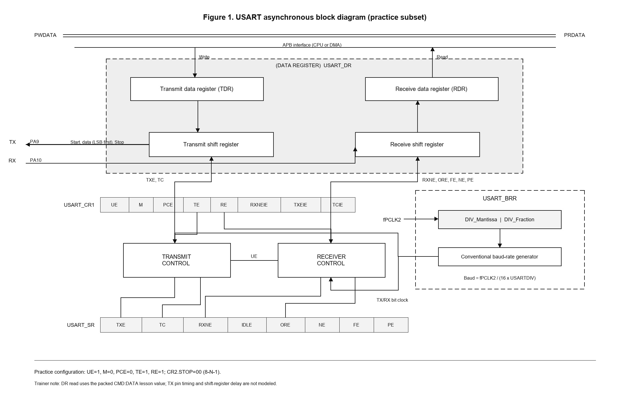
Figure 1. Practice-first USART1 data path: clock, CR1 enables, BRR, DR, shift registers, and SR flags
Source reconstruction from RM0008 Rev 21 Figure 279, Sections 27.3.2-27.3.4, RCC/AFIO controls, and DS5319 Rev 20, Table 5. The vendor figure was reduced to the first-lab lanes; special modes, DMA, flow control, and interrupt routing were intentionally omitted.
On the official device, TX writes go through USART_DR into the transmit shift register and drive PA9 / USART1_TX when the peripheral, transmitter, and pin path are enabled. RX samples PA10 / USART1_RX, loads USART_DR, and sets SR.RXNE until software reads the data register.
The trainer models a lesson-specific receive frame as CMD:DATA packed into USART1_DR. A modeled USART1_DR read consumes RX data. Writing USART1_DR records the low byte as trainer transmit data and leaves SR.TXE and SR.TC set after the immediate simulated transmission.
2.2 Read one frame as 8-N-1
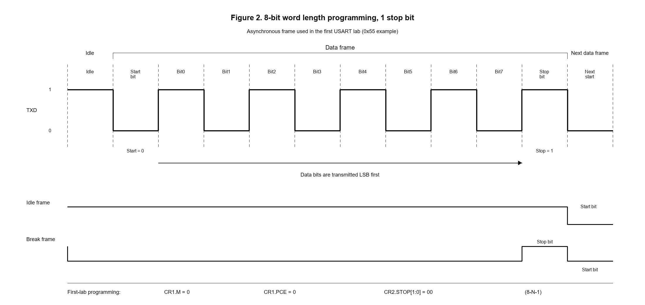
Figure 2. First-lab 8-N-1 frame using 0x55 as the LSB-first example byte
Source reconstruction from RM0008 Rev 21 Figure 280 and Section 27.3.1. Only the asynchronous 8-bit, no-parity, one-stop-bit path used by the lab is shown.
| Setting | Official STM32F103 meaning | Current Trainer boundary |
|---|---|---|
| CR1.M = 0 | One start bit, 8-bit word, selected stop-bit length. | Waveform display is fixed to eight data bits. |
| CR1.PCE = 0 | Parity generation and checking are disabled. | Parity selection/checking is not modeled. |
| CR2.STOP = 00 | One stop bit. | CR2 is not exposed; the displayed frame is fixed to one stop bit. |
When parity is enabled on the real device, parity occupies the word length: M=0 gives seven data bits plus parity, while M=1 gives eight data bits plus parity.
2.3 Use TXE for the next byte and TC for the final finish
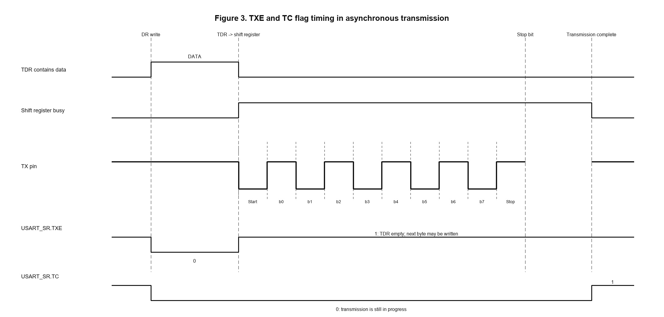
Figure 3. TXE becomes ready before TC becomes complete
Source reconstruction from RM0008 Rev 21 Sections 27.3.2 and 27.6.1. The timeline isolates the TDR, shift-register, TX pin, TXE, and TC relationship from the full USART block.
| Flag | Question it answers | Use it when | Current Trainer boundary |
|---|---|---|---|
| TXE | Is the transmit data register empty? | Before writing the next byte to USART1_DR. | The compact runtime has no shift-register busy interval. A modeled DR write is completed immediately and both flags remain set. |
| TC | Did the shift register send the stop bit completely? | Before disabling USART or changing a half-duplex direction on real hardware. |
3 Clock and pin routing
| Layer | Official STM32F103 fact | Current trainer contract |
|---|---|---|
| Clock | USART1 is on APB2. Enable USART1EN for the peripheral and IOPAEN for default PA9/PA10 GPIO configuration. AFIOEN is required only when software accesses AFIO registers, including remap control. | The fixed PA9/PA10 trainer route enforces USART1EN, IOPAEN, the matching GPIOA_CRH pad mode, a nonzero BRR, and the relevant CR1 enable bits. AFIO remapping remains reference-only. |
| GPIO | PA9 is TX alternate-function output and PA10 is RX input by default. Remapping to PB6/PB7 requires AFIOEN, IOPBEN, and a write to AFIO_MAPR.USART1_REMAP. | The board exposes the fixed independent External UART TX → PA10 / USART1_RX / UART_RX receive route. PB0 NTC sensing is a separate ADC1_IN8 path. |
| Baud | For oversampling by 16, USARTDIV = fCK / (16 * baud); BRR stores mantissa and fraction. | USART1_BRR must be nonzero and is visible in Registers and Code Watch. The common 72 MHz / 9600 bps setup uses 0x1D4C; animation timing is not derived from the programmed divider. |
| Interrupts | USART status flags can drive interrupt requests when enabled. | The trainer exposes flags and logs; current exercises use polling. |
3.1 PA9 / PA10 GPIO nibble values
| Pin / official signal | Register | Field / bit | Official value meaning | Current trainer result |
|---|---|---|---|---|
| PA9 / USART1_TX | GPIOA_CRH | CNF9[7:6] / MODE9[5:4] | Figure 1 drives the TX pad through the alternate-function output path. CNF9=10 selects alternate-function push-pull output. MODE9=10 means output mode, max 2 MHz; MODE9=11 means output mode, max 50 MHz. | A Trainer TX log entry requires PA9 alternate-function output mode together with IOPAEN, USART1EN, nonzero BRR, UE, and TE. The separate PA9 physical waveform is not drawn. |
| PA10 / USART1_RX | GPIOA_CRH | CNF10[11:10] / MODE10[9:8] | Figure 1 samples the RX pad through the input path. MODE10=00 selects input mode. CNF10=01 means floating input; CNF10=10 means pull-up/down input and uses ODR10 for pull direction. | The fixed independent External UART TX → PA10 / UART_RX route accepts a frame only when PA10 is a digital input and IOPAEN, USART1EN, nonzero BRR, UE, and RE are active. |
| Current code / value | Datasheet field interpreted as | Trainer에서 확인 |
|---|---|---|
| GPIOA_CRH[7:4] = 0xB (1011) | GPIOA_CRH.CNF9[7:6] = 10 and MODE9[5:4] = 11, so PA9 is alternate-function push-pull output at max 50 MHz. | This nibble is required before a USART1_DR write is accepted into the Trainer TX log. |
| GPIOA_CRH[11:8] = 0x4 (0100) | GPIOA_CRH.CNF10[11:10] = 01 and MODE10[9:8] = 00, so PA10 is a floating input. | This or the pull-input form is required for independent PA10 / UART_RX command frames. |
See the GPIO Register Datasheet for the complete nibble table.
3.2 Clock gates for default and remapped pins
| Route | Required clock gates | AFIO register action | Current trainer boundary |
|---|---|---|---|
| Default PA9/PA10 | IOPAEN=1 for GPIOA configuration; USART1EN=1 for USART1. | None. Do not add AFIOEN merely because PA9 is an alternate-function output. | The trainer enforces only USART1EN and CR1 RX/TX enables for its fixed route. |
| Remapped PB6/PB7 | IOPBEN=1, USART1EN=1, and AFIOEN=1. | Set AFIO_MAPR.USART1_REMAP=1. | Reference-only; the focused header/runtime does not expose or enforce the remap path. |
4 Register map and reset values
The complete block below follows RM0008 Rev 21 Table 198. Absolute addresses use USART1 base 0x40013800 + offset; trainer aliases do not change the official offsets.
| Offset | Register | Absolute address | Official reset | Official purpose / trainer boundary | Trainer 지원 여부 |
|---|---|---|---|---|---|
| 0x00 | USART1_SR | 0x40013800 | 0x000000C0 | Status register. The trainer models RXNE, TXE, TC, and a limited FE path. | 지원됨 |
| 0x04 | USART1_DR | 0x40013804 | Undefined | Data register. RM0008 Table 198 draws a zero reset row, but Section 27.6.2 is the reset authority; the trainer separately initializes modeled storage to zero. | 지원됨 |
| 0x08 | USART1_BRR | 0x40013808 | 0x00000000 | Baud-rate divider register. The trainer rejects RX/TX while BRR is zero; a nonzero value enables the simplified path but does not alter the UI animation timing. | 지원됨 |
| 0x0C | USART1_CR1 | 0x4001380C | 0x00000000 | Control register 1. The trainer acts on official UE, TE, and RE; bit 0 remains a legacy RX alias only. | 지원됨 |
| 0x10 | USART1_CR2 | 0x40013810 | 0x00000000 | Clock, stop-bit, LIN, and address controls for the full device. The current trainer header/MMIO list omits this register. | 미지원 |
| 0x14 | USART1_CR3 | 0x40013814 | 0x00000000 | DMA, flow-control, IrDA, smartcard, and advanced error controls. The current trainer header/MMIO list omits this register. | 미지원 |
| 0x18 | USART1_GTPR | 0x40013818 | 0x00000000 | Guard-time and prescaler register for smartcard/IrDA paths. The current trainer header/MMIO list omits this register. | 미지원 |
The USART1_DR reset discrepancy is handled in the owning register subsection below: the detailed RM0008 register description is the reset authority, while the trainer deterministic zero is a separate support fact.
4.1 Datasheet fields to current code and legacy executable aliases
Legacy executable aliases are kept only as a current-code compatibility bridge. No separate Registers alias row is rendered.
| Current code / value | Datasheet field interpreted as | Trainer에서 확인 |
|---|---|---|
| USART1_ISR | Legacy executable alias for USART1_SR at offset 0x00. | No separate Registers row is rendered; new code should prefer USART1_SR. |
| USART1_RDR | Legacy executable alias for USART1_DR at offset 0x04. | A read consumes the same modeled receive word as USART1_DR. |
| USART1->BRR = 0x1D4C | USART1_BRR.DIV_Mantissa[15:4] and DIV_Fraction[3:0] encode 72 MHz / 9600 bps in the reference setup. | Use Registers or Code Watch to confirm the stored nonzero value. BRR gates the simplified RX/TX path but does not alter the trainer animation timing. |
| USART1->CR1 = UE | TE | RE | USART1_CR1.UE[13], TE[3], and RE[2]. | RX frames are accepted when USART1EN, UE, and RE are set; DR TX writes are accepted when USART1EN, UE, and TE are set. |
| USART1_CR1_LEGACY_RXEN | Trainer-only compatibility alias over official USART1_CR1.SBK[0]. | Old lessons can still receive frames, but new code should use UE | RE. |
| USART1->CR2 / USART1->CR3 | Official frame-format and advanced-control registers. | Reference-only on real STM32F103; not exposed by the focused trainer header/MMIO contract. |
5 Register descriptions
5.1 Control register 1 (USART1_CR1)
Address offset: 0x0C Address: 0x4001380C Reset value: 0x00000000
| 31 | 30 | 29 | 28 | 27 | 26 | 25 | 24 | 23 | 22 | 21 | 20 | 19 | 18 | 17 | 16 | 15 | 14 | 13 | 12 | 11 | 10 | 9 | 8 | 7 | 6 | 5 | 4 | 3 | 2 | 1 | 0 |
|---|---|---|---|---|---|---|---|---|---|---|---|---|---|---|---|---|---|---|---|---|---|---|---|---|---|---|---|---|---|---|---|
| Reserved | UE | Other official CR1 control fields | TE | RE | RWU | SBK RXEN alias | |||||||||||||||||||||||||
| - | R/W | R/W | R/W | R/W | R/W | R/W | |||||||||||||||||||||||||
UE bit 13 enables USART1, TE bit 3 enables transmit, and RE bit 2 enables receive. Official bit 0 is SBK; the trainer also accepts it as a legacy RX enable alias, so new code should use UE | RE.
| Bit | Name | Access / values | Meaning | Current trainer register-value behavior |
|---|---|---|---|---|
| 31:14 | Reserved | - | Reserved, 사용하지 않음; keep at reset value 0. | - |
| 13 | UE | rw; 0 = USART prescaler/outputs disabled, 1 = USART enabled | Figure 1 turns the whole USART block on after configuration. | Required together with RE for RX and with TE for TX. |
| 12 | M | rw; 0 = 1 start + 8 data + stop, 1 = 1 start + 9 data + stop | Figure 1 selects the word length moved through the data path. | Reference-only; trainer packed frame uses its own CMD:DATA overlay. |
| 11 | WAKE | rw; 0 = Idle line wakeup, 1 = Address mark wakeup | Selects how a muted receiver wakes up. | Reference-only; mute/wakeup behavior is not modeled. |
| 10 | PCE | rw; 0 = parity disabled, 1 = parity enabled | Figure 1 inserts/checks a parity bit when enabled. | Reference-only; parity generation/checking is not modeled. |
| 9 | PS | rw; 0 = even parity, 1 = odd parity | Selects parity type when PCE=1. | Reference-only; parity generation/checking is not modeled. |
| 8 | PEIE | rw; 0 = interrupt inhibited, 1 = interrupt when PE=1 | Connects the parity-error flag to the USART interrupt request. | Reference-only; current exercises use polling. |
| 7 | TXEIE | rw; 0 = interrupt inhibited, 1 = interrupt when TXE=1 | Connects the transmit-data-empty flag to the USART interrupt request. | Reference-only; the trainer exposes flags and logs, not the full USART interrupt route. |
| 6 | TCIE | rw; 0 = interrupt inhibited, 1 = interrupt when TC=1 | Connects the transmission-complete flag to the USART interrupt request. | Reference-only; the trainer exposes flags and logs, not the full USART interrupt route. |
| 5 | RXNEIE | rw; 0 = interrupt inhibited, 1 = interrupt when RXNE=1 or ORE=1 | Connects receive-ready/overrun status to the USART interrupt request. | Reference-only; receive is polled through USART1_SR.RXNE. |
| 4 | IDLEIE | rw; 0 = interrupt inhibited, 1 = interrupt when IDLE=1 | Connects idle-line detection to the USART interrupt request. | Reference-only; IDLE detection is not modeled. |
| 3 | TE | rw; 0 = transmitter disabled, 1 = transmitter enabled | Figure 1 enables the TX block so writes to USART_DR can move toward TX. | Required with UE and USART1EN before a DR write records the low byte as trainer transmit data. |
| 2 | RE | rw; 0 = receiver disabled, 1 = receiver enabled and searching for a start bit | Figure 1 enables the RX block so PA10 data can be accepted. | Required with UE and USART1EN before modeled receive frames are accepted. |
| 1 | RWU | rw; 0 = receiver active, 1 = receiver in mute mode | Controls receiver wakeup/mute behavior. | Reference-only; mute/wakeup behavior is not modeled. |
| 0 | SBK | rw; 0 = no break, 1 = send break | Official hardware sends a break character when set. | The trainer also treats bit 0 as the legacy RXEN alias for old lessons. New code must use UE | RE. |
5.2 Status register (USART1_SR)
Address offset: 0x00 Address: 0x40013800 Reset value: 0x000000C0
| 31 | 30 | 29 | 28 | 27 | 26 | 25 | 24 | 23 | 22 | 21 | 20 | 19 | 18 | 17 | 16 | 15 | 14 | 13 | 12 | 11 | 10 | 9 | 8 | 7 | 6 | 5 | 4 | 3 | 2 | 1 | 0 |
|---|---|---|---|---|---|---|---|---|---|---|---|---|---|---|---|---|---|---|---|---|---|---|---|---|---|---|---|---|---|---|---|
| Reserved | CTS | LBD | TXE | TC | RX NE | ID LE | ORE | NE | FE | PE RX alias | |||||||||||||||||||||
| - | rc_ w0 | rc_ w0 | R | rc_ w0 | rc_ w0 | R | R | R | R | R | |||||||||||||||||||||
rc_w0 means read/clear by writing 0; writing 1 does not clear the official flag. Error/idle flags marked R are cleared by the documented status-then-data read sequence, not by treating the entire register as ordinary read-only storage.
| Bit | Field | Official access / values | Figure block and official meaning | Official clear sequence | Current trainer behavior |
|---|---|---|---|---|---|
| 31:10 | Reserved | - | Reserved, 사용하지 않음; forced to 0 on official hardware. | - | - |
| 9 | CTS | rc_w0; 0 = no CTS change, 1 = CTS toggled while CTSE=1 | Figure 1 flow-control side path reports a CTS input toggle. | Write 0 to CTS. | Reference-only; CTS flow control and field-specific rc_w0 behavior are not modeled. |
| 8 | LBD | rc_w0; 0 = LIN break not detected, 1 = LIN break detected | LIN break detection reports a break condition on the receive path. | Write 0 to LBD. | Reference-only; LIN detection and field-specific rc_w0 behavior are not modeled. |
| 7 | TXE | R; 0 = data not transferred to shift register, 1 = data transferred | Figure 1 transmit data register is empty enough for software to write the next byte. | Write USART_DR. | Reset set. An accepted DR write is transmitted immediately in the model and leaves TXE=1; no shift-register busy interval is simulated. |
| 6 | TC | rc_w0; 0 = transmission not complete, 1 = transmission complete | Figure 1 transmit shift register has finished the frame and TXE is also set. | Read USART_SR, then write USART_DR; writing 0 to TC also clears it. | Reset set. An accepted DR write leaves TC=1; the official SR-read/DR-write clearing sequence is not modeled. |
| 5 | RXNE | rc_w0; 0 = data not received, 1 = received data ready | Figure 1 receive shift register has transferred a word into USART_DR. | Read USART_DR; writing 0 to RXNE also clears it. | An accepted modeled receive frame sets RXNE. A modeled DR read clears RXNE plus the legacy bit-0 ready alias. |
| 4 | IDLE | R; 0 = no idle line detected, 1 = idle line detected | The receiver detected an idle line after prior receive activity. | Read USART_SR, then read USART_DR. | Reference-only; IDLE detection and its sequence are not modeled. |
| 3 | ORE | R; 0 = no overrun, 1 = overrun detected | The receiver got a new word while RXNE was already set. | Read USART_SR, then read USART_DR. | Reference-only; receive overrun generation and its clear sequence are not modeled. |
| 2 | NE | R; 0 = no noise detected, 1 = noise detected | The receiver detected noise in a received frame. | Read USART_SR, then read USART_DR. | Reference-only; noise detection is not modeled. |
| 1 | FE | R; 0 = no framing error, 1 = framing error or break detected | The receiver sampled a frame with an invalid stop-bit/framing condition. | Read USART_SR, then read USART_DR. | The trainer sets FE when a modeled receive frame is rejected because the USART clock/RX enable path is disabled; a later accepted frame clears it. The official read sequence is not modeled. |
| 0 | PE | R; 0 = no parity error, 1 = parity error detected | The receiver detected a parity mismatch after parity checking. | After RXNE is set, read USART_SR, then read USART_DR. | The trainer overlays bit 0 as a legacy RX-ready flag, so official PE behavior is not represented by this bit in the compact runtime. |
The focused MMIO accepts a stored SR word but does not reproduce official per-field rc_w0 masking. Do not teach raw SR writes as the trainer equivalent of RM0008 clearing rules; use USART1_DR read for the supported RX consume path.
5.3 Data register (USART1_DR)
Address offset: 0x04 Address: 0x40013804 Official reset value: Undefined. Current trainer initialization: 0x00000000.
RM0008 Table 198 draws a zero reset row for the map summary, while the detailed Section 27.6.2 register description states Reset value: Undefined. Firmware should not read DR before RXNE or assume power-on contents. The trainer's zero initialization is deterministic UI state, not official silicon reset behavior.
| Field | Name | Access / values | Meaning | Current trainer register-value behavior |
|---|---|---|---|---|
| 31:9 | Reserved | - | Reserved and forced to 0 on official hardware. | Trainer RX word bits 15:9 carry CMD[7:1]; bits 31:16 remain unused. This is an intentional trainer overlay. |
| 8 | DR[8] | rw; ninth data bit when M=1 | Ninth data bit in official 9-bit word-length mode. | Trainer RX word bit 8 carries CMD[0]; this is a trainer overlay, not an official command field. |
| 7:0 | DR[7:0] | rw; receive read / transmit write | Lower receive data when read; lower transmit data when written. | A modeled DR read returns the packed CMD:DATA word and clears RXNE; bits 7:0 are DATA. A modeled DR write records its low byte as trainer transmit data. |
5.4 Baud-rate register (USART1_BRR)
Address offset: 0x08 Address: 0x40013808 Reset value: 0x00000000
In official oversampling-by-16 mode, USARTDIV = fCK / (16 * baud) and BRR stores mantissa and fraction fields. For a 72 MHz USART clock and 9600 bps, USARTDIV = 468.75 and the common reference value is 0x1D4C. The trainer requires this register to be nonzero, while the UI keeps a 9600 bps protocol label and uses display animation timing that is not derived from BRR.
| Bits | Field | Access / reset | 0 or programmed value | Configuration note | Trainer behavior |
|---|---|---|---|---|---|
| 15:4 | DIV_Mantissa[11:0] | R/W / 0 | Integer part of USARTDIV; together with the fraction, 0x1D4C represents 468.75 for 72 MHz / 9600 bps. | Program before enabling normal TX/RX operation. | Stored in modeled USART1_BRR; it does not affect trainer waveform timing. |
| 3:0 | DIV_Fraction[3:0] | R/W / 0 | Fractional sixteenth of USARTDIV. | The official baud counters stop for the disabled TE or RE direction. | Stored; the trainer's 9600 bps label and display animation are not recalculated from this field. |
5.5 Reference-only USART control registers (USART1_CR2, USART1_CR3, USART1_GTPR)
These registers are official RM0008 USART1 registers. The current trainer does not expose them through the focused USART_TypeDef, MMIO list, or Registers view.
| Register | Field | Access / values | Meaning | Current trainer register-value behavior |
|---|---|---|---|---|
| USART1_CR2 | Reserved | - | Reserved, 사용하지 않음; keep at reset value 0. | Reference-only; not exposed by the current trainer header/MMIO contract. |
| USART1_CR2 | LINEN[14] | rw; 0 = LIN mode disabled, 1 = LIN mode enabled | Enables LIN break generation/detection around the USART data path. | Reference-only; LIN is not modeled. |
| USART1_CR2 | STOP[13:12] | rw; 00 = 1 stop bit, 01 = 0.5 stop bit, 10 = 2 stop bits, 11 = 1.5 stop bit | Selects how many stop bits are appended or checked for each frame. | Reference-only; trainer frames use fixed 1-stop-bit UART timing. |
| USART1_CR2 | CLKEN[11] | rw; 0 = CK pin disabled, 1 = CK pin enabled | Enables the synchronous clock output path. | Reference-only; synchronous clock pin behavior is not modeled. |
| USART1_CR2 | CPOL[10] | rw; 0 = steady low clock, 1 = steady high clock | Selects synchronous clock polarity when CLKEN=1. | Reference-only; synchronous clock pin behavior is not modeled. |
| USART1_CR2 | CPHA[9] | rw; 0 = first clock transition captures, 1 = second clock transition captures | Selects synchronous clock phase. | Reference-only; synchronous clock pin behavior is not modeled. |
| USART1_CR2 | LBCL[8] | rw; 0 = last bit clock pulse not output, 1 = last bit clock pulse output | Controls whether the last transmitted data bit also produces a clock pulse. | Reference-only; synchronous clock pin behavior is not modeled. |
| USART1_CR2 | LBDIE[6] | rw; 0 = interrupt inhibited, 1 = interrupt when LBD=1 | Connects LIN break detection to the USART interrupt request. | Reference-only; USART interrupt route is not modeled. |
| USART1_CR2 | LBDL[5] | rw; 0 = 10-bit break detection, 1 = 11-bit break detection | Selects LIN break detection length. | Reference-only; LIN is not modeled. |
| USART1_CR2 | ADD[3:0] | rw; 0000-1111 = USART node address | Stores the multiprocessor address used for address-mark wakeup. | Reference-only; multiprocessor wakeup is not modeled. |
| USART1_CR3 | Reserved | - | Reserved, 사용하지 않음; keep at reset value 0. | Reference-only; not exposed by the current trainer header/MMIO contract. |
| USART1_CR3 | CTSIE[10] | rw; 0 = interrupt inhibited, 1 = interrupt when CTS=1 | Connects CTS status changes to the USART interrupt request. | Reference-only; flow-control interrupt behavior is not modeled. |
| USART1_CR3 | CTSE[9] | rw; 0 = CTS flow control disabled, 1 = CTS mode enabled | Stops or resumes transmitter output based on the CTS input. | Reference-only; CTS flow control is not modeled. |
| USART1_CR3 | RTSE[8] | rw; 0 = RTS flow control disabled, 1 = RTS mode enabled | Drives the RTS output to tell an external transmitter whether the receiver can accept data. | Reference-only; RTS flow control is not modeled. |
| USART1_CR3 | DMAT[7] | rw; 0 = transmitter DMA disabled, 1 = transmitter DMA enabled | Requests DMA service when transmit data can be loaded. | Reference-only; USART DMA is not modeled. |
| USART1_CR3 | DMAR[6] | rw; 0 = receiver DMA disabled, 1 = receiver DMA enabled | Requests DMA service when receive data is ready. | Reference-only; USART DMA is not modeled. |
| USART1_CR3 | SCEN[5] | rw; 0 = smartcard mode disabled, 1 = smartcard mode enabled | Enables smartcard protocol behavior. | Reference-only; smartcard behavior is not modeled. |
| USART1_CR3 | NACK[4] | rw; 0 = NACK transmission disabled, 1 = NACK transmission enabled | Controls smartcard NACK generation on parity error. | Reference-only; smartcard behavior is not modeled. |
| USART1_CR3 | HDSEL[3] | rw; 0 = half-duplex not selected, 1 = half-duplex selected | Uses a single bidirectional data line instead of separate TX/RX lines. | Reference-only; half-duplex behavior is not modeled. |
| USART1_CR3 | IRLP[2] | rw; 0 = normal IrDA mode, 1 = low-power IrDA mode | Selects IrDA low-power timing when IrDA is enabled. | Reference-only; IrDA behavior is not modeled. |
| USART1_CR3 | IREN[1] | rw; 0 = IrDA disabled, 1 = IrDA enabled | Enables IrDA modulation/demodulation. | Reference-only; IrDA behavior is not modeled. |
| USART1_CR3 | EIE[0] | rw; 0 = error interrupt inhibited, 1 = error interrupt enabled for FE/ORE/NE with DMAR | Connects advanced receive errors to the interrupt request in multi-buffer communication. | Reference-only; trainer does not emulate USART error interrupts. |
| USART1_GTPR | GT[15:8] | rw; 0x00-0xFF = guard time value | Defines smartcard guard time. | Reference-only; not exposed by the current trainer header/MMIO contract. |
| USART1_GTPR | PSC[7:0] | rw; 0x00-0xFF = prescaler value | Defines the smartcard/IrDA prescaler. | Reference-only; not exposed by the current trainer header/MMIO contract. |
6 Student register guide and code examples
6.1 Current trainer code example
- For the current RX-only example, enable IOPAEN and USART1EN, then configure PA10 as input. PA9 remains official TX reference truth but is not initialized by the executable example.
- Enable AFIOEN only before accessing AFIO_MAPR for the PB6/PB7 remap; that remap path is not exposed by the focused trainer header.
- Read the real pin truth as PA9 alternate-function output and PA10 input. The fixed Trainer route enforces those GPIOA_CRH modes; the receive example uses independent External UART TX → PA10 / UART_RX.
- Write USART1_BRR before enabling the USART in F103-style setup code.
- Set only USART1_CR1.UE and USART1_CR1.RE. The executable example leaves TE=0 and never writes USART1_DR.
- Poll USART1_SR.RXNE, then use USART1_DR read to consume the Trainer frame and execute the modeled read side effect.
| Receive boundary | Official STM32F103 | Current Trainer |
|---|---|---|
| Data returned by one DR read | DR[8:0] contains one received 8/9-bit data word. A two-byte application message requires two receive events and two DR reads. | The panel still renders CMD and DATA as two consecutive 8-N-1 bytes, but the simulator places CMD[15:8]:DATA[7:0] in one modeled DR value and raises RXNE once. |
| Example portability | Store CMD after the first RXNE/DR sequence, then store DATA after the second sequence before decoding the application message. | The frame >> 8 example below is executable only against the Trainer packed-frame contract and must not be copied unchanged to a real STM32F103. |
void user_init(void)
{
    trainer_clock_init_72mhz();
    RCC->APB2ENR = RCC_APB2ENR_AFIOEN | RCC_APB2ENR_IOPAEN | RCC_APB2ENR_IOPBEN | RCC_APB2ENR_ADC1EN;
    RCC->APB2ENR |= RCC_APB2ENR_USART1EN;
    RCC->APB1ENR = RCC_APB1ENR_TIM2EN;
    GPIOA->CRH = (GPIOA->CRH & ~(0xFu << 8)) | (0x4u << 8); /* PA10 RX */
    USART1->BRR = 0x1D4Cu;
    USART1->CR1 = USART1_CR1_UE | USART1_CR1_RE;
}

void user_loop(void)
{
    if ((read_reg(USART1_SR) & (1u << 5)) != 0u) {
        uint32_t frame = read_reg(USART1_DR); /* Trainer-only CMD:DATA packed word */
        uint32_t cmd = (frame >> 8) & 0xFFu;
        uint32_t data = frame & 0xFFu;
        watch_u32("uart_cmd", cmd);
        watch_u32("uart_data", data);
    }
}
Read this flow as IOPAEN + USART1EN -> PA10 input -> BRR -> UE/RE -> RXNE poll -> DR read. The register-value behavior above is enough to review USART1 code; learner-facing UI confirmation is mapped in the USART1/UART User Description.
6.2 Full STM32F103 example when every USART register is available
Reference-only on real STM32F103: The focused trainer header omits USART1_CR2 and USART1_CR3, and the trainer does not model full pin muxing or hardware polling delays. Use Section 6.1 for executable trainer code.
- Keep the same core bring-up path: RCC->APB2ENR.USART1EN, BRR, and CR1.
- Use the official pin truth: PA9 = USART1_TX and PA10 = USART1_RX, with optional remap to PB6/PB7.
- Expand into frame-format and stop-bit control through CR2 and advanced flow control through CR3 when the full device path needs them.
RCC->APB2ENR |= (1u << 2);   /* IOPAEN: default PA9/PA10 path */
RCC->APB2ENR |= (1u << 14);  /* USART1EN */

/* Official STM32F103 pin setup example */
GPIOA->CRH &= ~((0xFu << 4) | (0xFu << 8));
GPIOA->CRH |=  (0xBu << 4);   /* PA9  AF push-pull */
GPIOA->CRH |=  (0x4u << 8);   /* PA10 floating input */

USART1->BRR = 0x1D4Cu;
USART1->CR1 = (1u << 13) | (1u << 3) | (1u << 2);  /* UE | TE | RE */
USART1->CR2 = 0u;                                      /* 1 stop bit */
USART1->CR3 = 0u;                                      /* no flow control */

while ((USART1->SR & (1u << 7)) == 0u) { }            /* TXE */
USART1->DR = 'A';
while ((USART1->SR & (1u << 6)) == 0u) { }            /* TC */
This full example uses the default PA9/PA10 mapping, so it does not enable AFIO. For PB6/PB7 remap, first enable AFIOEN and IOPBEN, then write AFIO_MAPR.USART1_REMAP and configure GPIOB. That remap setup is reference-only in the focused trainer.
6.3 Simulator alignment notes
| View | Expected wording or behavior |
|---|---|
| Board · System route | External UART TX → PA10 / USART1_RX / UART_RX shows receive waveform state and USART1_SR.RXNE relation. PB0 NTC is verified separately in ADC surfaces. |
| Registers | The focused list renders GPIOA_CRH, USART1_BRR, USART1_CR1, USART1_SR, and USART1_DR. Confirm DR read/write side effects in Docs / Log. Legacy USART1_ISR/USART1_RDR remain aliases only. |
| Modeled receive/transmit behavior | RX input sets RXNE and updates DR. Modeled DR reads clear RXNE. DR writes record trainer transmit bytes and leave TXE/TC set. |
| Mission | RX enable may pass through official UE|RE or the legacy bit 0 alias, but new examples should use the official F103 bits. |