VMD-MD01-Lite Motor Driver Datasheet
Control/observe signal guide for EN, DIR, PWM, FAULT_IN, CURRENT_SENSE, and H-bridge output paths
Contents
- General description
- Trainer signal summary
- Main features
- Mode-specific trainer schematics
- Pin description
- Operating states
- Input-to-output truth table and waveforms
- Fault indication and reset
- Student application notes
1 General description
VMD-MD01-Lite is an H-bridge motor-driver device intended for low-channel-count electromechanical actuation systems. The device receives an enable command, a direction command and a PWM drive command from an external controller, and converts these signals into a bidirectional power output across the motor terminals.
In addition to the power-output function, the driver monitors fault conditions and publishes a digital fault output. A current feedback path is also provided so that the system controller can observe load behavior or detect abnormal operating conditions.
This document is not the register chapter. The GPIOA, TIM2, and ADC1 chapters explain how the MCU produces or reads each signal; this chapter explains what each board-facing motor-driver signal means after those registers are set.
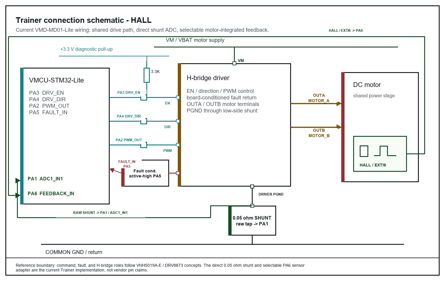
Figure 1A. HALL tab: shared drive path, Kelvin-connected 0.05 Ω shunt to PA1, and motor-integrated 3.3 V pull-up HALL_IN to PA6 / EXTI6
Source boundary: H-bridge command, output, and fault roles are reconstructed from ST VNH5019A-E and TI DRV8873 concepts. The raw low-side shunt and 3.3 V open-collector Hall adapter are the current Trainer implementation, not vendor pin claims. AFIO_EXTICR2.EXTI6=0000 selects PA6; other port sources and Hall transition counts are reference-only/Trainer plant assumptions because no Hall vendor device is selected.
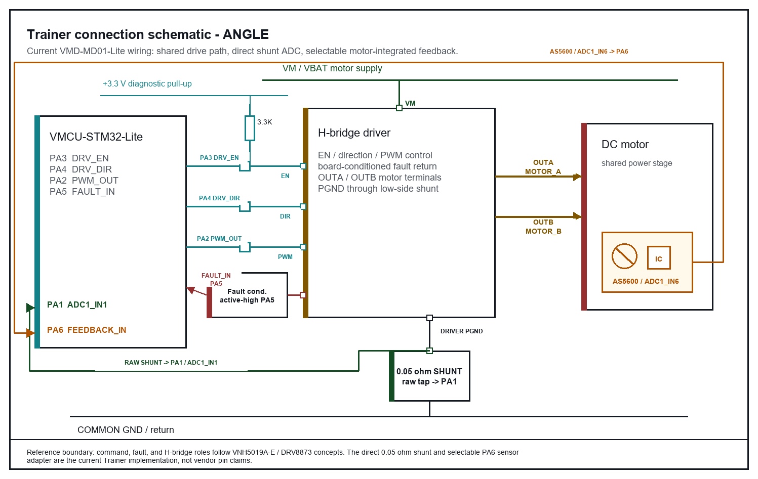
Figure 1B. ANGLE tab: the same MCU, driver, motor, and shunt with only the feedback adapter changed to 3.3 V AS5600 analog OUT → PA6 / ADC1_IN6
Source boundary: the common AS5600 profile is 3.3 V mode, OUTS=00, and programmed MANG=180°, yielding 2048 distinct DAC steps across 0..180°. I²C programming, DIR, PWM output, and magnet diagnostics remain reference-only. The driver path and firmware remain shared with Figure 1A.
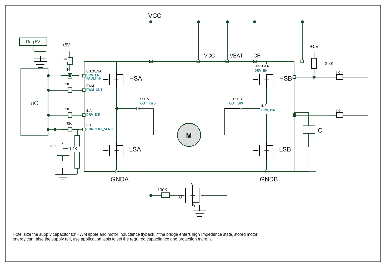
Figure 2. Reconstructed driver IC application circuit with ST-style support components, DIAG/EN, CS, OUTA/OUTB, VCC, VBAT, CP, GND, and motor load
Source reconstruction: ST VNH5019A-E Figure 5 on page 16, typical application circuit for DC to 20 kHz PWM operation with reverse-battery protection. Teal labels show the trainer-facing aliases; no vendor artwork is pasted.
2 Trainer signal summary
| Signal | MCU route | Student meaning |
|---|---|---|
| DRV_EN | PA3 / GPIOA_ODR bit3 | HIGH enables the driver. LOW stops drive output. |
| DRV_DIR | PA4 / GPIOA_ODR bit4 | LOW = CW, HIGH = CCW. |
| PWM_OUT | PA2 / PWM_OUT trainer route; TIM2_CCR1 duty command | 0/3.3 V MCU logic duty command. This is not official TIM2_CH1 pin mapping; STM32F103 PA2 is TIM2_CH3. |
| FAULT_IN | PA5 / GPIOA_IDR bit5 | Board-conditioned active-high 3.3 V digital input. HIGH means fault; stop the driver and set PWM to 0. Fault causes are manually injected by the current Trainer. |
| CURRENT_SENSE | PA1 / ADC1_IN1 / ADC_DR | Raw voltage from the 0.05 Ω low-side shunt, Kelvin-connected to PA1 for analog load-current feedback. Real hardware needs adequate I²R rating plus ADC RC/clamp protection; the Trainer-private ADC1_DR_CH1 name is a compatibility-only legacy alias. |
| OUT_FWD / MOTOR_A OUT_BW / MOTOR_B |
Graph / schematic output | H-bridge VM-domain power terminals. CW switches Motor A between 0 and VM while Motor B is 0 V; CCW switches Motor B while Motor A is 0 V. The selected average is D × VM, with VM=12 V by default. |
Reference drivers often expose a low-true nFAULT or DIAG pin and an IPROPI or CS current output. The board-facing MCU signal is intentionally named FAULT_IN. Driver control and conditioned fault logic use 0/3.3 V, PA1 / CURRENT_SENSE uses a 3.3 V ADC reference, and Motor A/B use the VM = 12 V power domain. The external PA10 UART alone retains a separate 0/5 V FT input contract. Source PDFs: VNH5019A-E and DRV8873-Q1.
3 Main features
- Single PWM input for proportional drive command
- Dedicated enable input and direction input
- Bidirectional H-bridge power stage with OUT_FWD and OUT_BW
- Board-facing digital fault input to the MCU, active high
- Direct 0.05 Ω low-side shunt sense path to ADC1 channel 1, with Kelvin/power/protection requirements for real hardware
- VM-domain Motor A/B output model: selected terminal average = D × VM; signed differential command = ±VM × D
- Support for stop, ready, running and fault operating states
4 Mode-specific trainer schematics
Figures 1A and 1B are the student-facing schematics for the two feedback tabs. Both keep the same MCU, H-bridge, motor, direct low-side shunt, fault path, and firmware contract. Only the motor-integrated PA6 feedback adapter changes.
| Reference datasheet element | Applied trainer signal | Why it is shown this way |
|---|---|---|
| DIAG/EN, nFAULT | DRV_EN command and active-high FAULT_IN return | Real drivers often use a shared enable/diagnostic or open-drain fault pin. The trainer separates the MCU command and board-conditioned fault input. |
| INA/INB, PH/EN, PWM | DRV_DIR, DRV_EN, PWM_OUT | The lab uses one enable, one direction, and one PWM command while preserving the H-bridge control idea. |
| CS / IPROPI | Reference comparison only; the active Trainer uses the raw 0.05 Ω shunt node into PA1 / ADC1_IN1 | Vendor CS/IPROPI explains the current-feedback concept, but the current Trainer does not route or amplify that pin. |
| OUTA/OUTB or OUT1/OUT2 | OUT_FWD / OUT_BW | The UI shows average VM-domain Motor A/B terminal voltage, not 3.3 V GPIO logic and not sub-cycle switching detail. |
5 Pin description
| Pin | Direction | Type | Description |
|---|---|---|---|
| PA3 / DRV_EN | MCU -> Driver | Digital | Active-high enable command for the Trainer driver output stage. |
| PA4 / DRV_DIR | MCU -> Driver | Digital | Direction command: LOW selects CW / OUT_FWD; HIGH selects CCW / OUT_BW. |
| PA2 / PWM_OUT | MCU -> Driver | Digital PWM | 0/3.3 V Trainer PWM command generated from TIM2_CCR1 duty. |
| PA5 / FAULT_IN | Driver -> MCU | Digital | Board-conditioned active-high 3.3 V diagnostic. It represents an inverted or conditioned form of the low-true reference nFAULT/DIAG output. |
| PA1 / CURRENT_SENSE / ADC1_IN1 | Shunt sense node -> MCU | Analog | Raw low-side shunt feedback follows Vshunt = I × 0.05 Ω and is Kelvin-connected to PA1, whose ADC range is 0..3.3 V. The normal drive model is load-dependent; manual overcurrent fault state may reach 8.5 A (0.425 V, about 3.61 W in the shunt). Real hardware must rate the resistor for I²R, keep PA1 within 0..VDDA, and add RC/clamp protection. |
| OUT_FWD / MOTOR_A | Driver -> Motor | Power | VM-domain terminal switched 0↔VM for CW; average D × VM. |
| OUT_BW / MOTOR_B | Driver -> Motor | Power | VM-domain terminal switched 0↔VM for CCW; average D × VM. |
| VM | Input | Power | Motor-supply rail. The current Trainer motor model defaults to 12 V. |
| GND | - | Power | Common return path |
6 Operating states
| State | Description |
|---|---|
| STOP | Effective drive disabled. The trainer displays both motor-output averages as 0.00 V; reference devices may implement brake or Hi-Z depending on mode. |
| READY | Device enabled and prepared for PWM-driven motion, but no effective drive applied |
| RUNNING / CW | DRV_EN = 1, DRV_DIR = 0, PWM duty > 0%; OUT_FWD is selected. |
| RUNNING / CCW | DRV_EN = 1, DRV_DIR = 1, PWM duty > 0%; OUT_BW is selected. |
| FAULT | FAULT_IN = HIGH; the effective Graph outputs are zero and firmware must write PWM = 0, then DRV_EN = LOW. |
7 Input-to-output truth table and waveforms
| DRV_EN | DRV_DIR | PWM duty | FAULT_IN | Driver state | OUT_FWD / MOTOR_A | OUT_BW / MOTOR_B | Signed motor command |
|---|---|---|---|---|---|---|---|
| 0 | X | X | 0 | STOP | 0 V | 0 V | 0 V |
| 1 | X | 0% | 0 | READY | 0 V | 0 V | 0 V |
| 1 | 0 | D% > 0% | 0 | RUNNING / CW | Switches 0↔VM; average = D × VM | 0 V | +VM x D |
| 1 | 1 | D% > 0% | 0 | RUNNING / CCW | 0 V | Switches 0↔VM; average = D × VM | -VM x D |
| X | X | X | 1 | FAULT | 0 V | 0 V | 0 V |
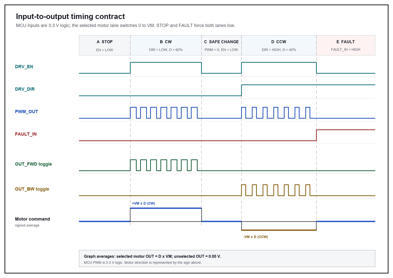
Figure 3. Input-to-output timing contract for STOP, CW, safe direction change, CCW, and FAULT
Source-derived layout: ST VNH5019A-E Figure 11 on pages 22-23 establishes the multi-lane input/PWM/output waveform reading order. Read input PWM/EN/DIR/FAULT lanes as 3.3 V logic and Motor A/B lanes as 0↔VM power switching; any legacy 5 V output-lane scale in the illustration is superseded by this VM-domain table. Timing is not copied vendor timing.
Figure 3 answers the literal HIGH/LOW sequence: EN LOW produces no output; EN HIGH + DIR LOW applies PWM-gated VM switching to Motor A; after PWM is set to zero, DIR HIGH applies the next PWM-gated VM switching to Motor B; FAULT_IN HIGH forces both effective outputs to zero. The Trainer does not model sub-cycle MOSFET dead time, recirculation, or detailed brake/coast current decay.
8 Fault indication and reset
Real reference drivers commonly expose an open-drain, low-true nFAULT or DIAG signal. The Trainer board contract inverts or conditions that signal so PA5 / FAULT_IN is active high: LOW means normal and HIGH means a conditioned 3.3 V fault. This board conversion is why the MCU-facing polarity differs from the source devices. Current fault classes are created only by manual Trainer injection; neither the raw shunt reading nor a simulated junction temperature automatically asserts them.
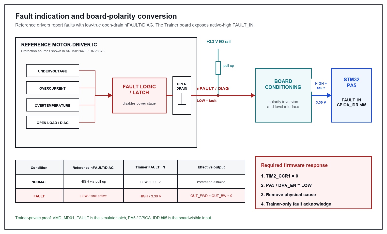
Figure 4. Reference low-true fault indication and Trainer active-high board conversion
Source reconstruction: VNH5019A-E Table 2 and pages 7-8 describe open-drain DIAG/EN fault reporting; page 16 Table 13 shows fault output action. DRV8873 Figure 17 on page 22 shows the nFAULT pull-up, and Table 13 on page 28 lists protection responses. The board-conditioning block is the local Trainer contract, not a claim about either vendor IC's internal circuit.
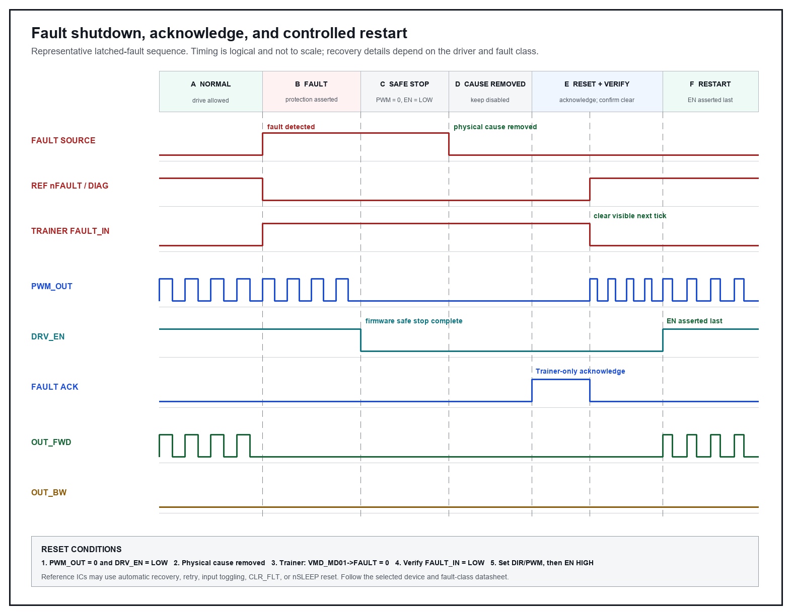
Figure 5. Representative fault shutdown, acknowledge, clear verification, and controlled restart timing
Source-derived layout: VNH5019A-E Figure 6 on page 17 establishes the fault-latch and input-transition reading order; DRV8873 Table 13 on page 28 shows that recovery can be automatic, retry-based, or latched by fault class and configuration. The FAULT ACK lane and next-tick PA5 confirmation are the current Trainer contract. Timing is logical and not to scale.
8.1 Reset and recovery behavior
| Device / surface | Fault indication | Recovery method | Required interpretation |
|---|---|---|---|
| ST VNH5019A-E reference | Faulted bridge leg is latched off and the associated DIAG/EN is pulled LOW. | After the fault is removed, the relevant input transition unlatches the output; the page-17 procedure applies to that device. | Reference behavior only. Do not map the shared DIAG/EN pin directly to Trainer PA5. |
| TI DRV8873 reference | Low-true open-drain nFAULT; bridge response depends on fault and configuration. | Recovery may be automatic, retry-based, or latched through CLR_FLT/nSLEEP. | Use the selected fault-class row in the vendor table; there is no universal reset pulse. |
| Current Trainer contract | Manual fault injection sets a board-conditioned 3.3 V PA5 / FAULT_IN = HIGH; both effective output probes are zero. | With PWM = 0 and EN = LOW, write VMD_MD01->FAULT = 0u, then verify the latch and PA5 are clear on a later tick. | The acknowledge neither repairs a physical fault nor re-enables the motor. |
8.2 Fault class mapping
| Fault class | Reference / Trainer meaning | Current Trainer exposure |
|---|---|---|
| overCurrent | Overcurrent or overload protection is present in both reference families, with device-specific current-limit and recovery behavior. | VMD_MD01_FAULT_OVERCURRENT / bit0, manual Trainer injection only; it is not calculated from PA1 or a vendor threshold |
| overTemperature | Thermal protection disables the reference output stage under device-specific conditions. | VMD_MD01_FAULT_OVERTEMP / bit1, manual Trainer injection only; no junction-temperature model is present |
| communicationError | Trainer system-level command-validity fault; not a VNH5019A-E or DRV8873 pin claim. | VMD_MD01_FAULT_COMM_ERROR / bit2, manual Trainer injection only |
| undervoltage / open load | Shown in the source devices' protection architecture and fault tables. | Reference-only as separate causes; no dedicated Trainer fault bit and no automatic threshold/recovery model |
8.3 Trainer reset sequence
| Figure 5 phase | Action | Required confirmation |
|---|---|---|
| B -> C | Safe stop: set PWM = 0 and DRV_EN = LOW. | TIM2_CCR1 = 0; PA3 output is LOW; OUT_FWD and OUT_BW are 0 V. |
| D | Real hardware: remove the physical fault cause while the output remains disabled. | Load, wiring, supply and thermal state are safe. |
| E | Trainer acknowledge: write VMD_MD01->FAULT = 0u. | The Trainer-private fault latch clears on the next simulator tick. |
| E | Confirm both exposed views are clear before preparing a command. | VMD_MD01_FAULT = 0 and PA5 / GPIOA_IDR bit5 is LOW. |
| E -> F | Set DIR and PWM deliberately, then assert DRV_EN last. | The restart direction and duty are intentional; output resumes only after EN is HIGH. |
/* 1) Safe stop first. */
TIM2->CCR1 = 0u;                    /* PA2 / PWM_OUT duty = 0% */
GPIOA->ODR &= ~GPIOA_DRV_EN_BIT;  /* PA3 / DRV_EN = LOW */

/* 2) Real hardware: remove the physical fault cause here. */

/* 3) Trainer-only acknowledge. The visible PA5 state updates on a later tick. */
VMD_MD01->FAULT = 0u;

/* 4-5) Restart only after both Trainer-visible fault views are clear. */
if ((VMD_MD01->FAULT == 0u) &&
    ((GPIOA->IDR & GPIOA_FAULT_IN_BIT) == 0u)) {
    GPIOA->ODR &= ~GPIOA_DRV_DIR_BIT; /* CW: DIR LOW */
    TIM2->CCR1 = 50u;                  /* 50% duty */
    GPIOA->ODR |= GPIOA_DRV_EN_BIT;    /* EN asserted last */
}9 Student application notes
This final section links the board-facing driver signals back to the student-visible register and UI workflow. In the current trainer flow, the controller drives DRV_EN, DRV_DIR, and PWM_OUT, then checks FAULT_IN, CURRENT_SENSE, OUT_FWD, and OUT_BW. In Graph, the observable H-bridge output probes are labeled OUT_FWD toggle and OUT_BW toggle; each probe shows an average beside its live value because the trainer does not model sub-cycle bridge switching.
The CURRENT_SENSE signal is the raw voltage at the 0.05 Ω low-side shunt and is connected to PA1 / ADC1_IN1 using Kelvin sense traces. Real hardware must rate shunt power, protect the ADC, and account for low-side ground lift and unobserved recirculation/reverse current. The FAULT_IN signal returns to PA5 as a board-conditioned active-high 3.3 V GPIO input; its current causes are manually injected.
Student reading order: identify the board-facing signal name here, follow its function in Figure 1A or 1B through Figure 5, then return to the GPIOA, TIM2, or ADC1 chapter to see which MCU register path produces or observes it.
| What to check now | What it proves | Related next chapter |
|---|---|---|
| DRV_EN, DRV_DIR, PWM_OUT | The controller is sending a valid command into the driver input side. | GPIOA and TIM2 PWM |
| OUT_FWD, OUT_BW | The H-bridge direction and VM-domain average terminal voltage match the command; Graph uses MOTOR_A / OUT_FWD and MOTOR_B / OUT_BW with D × VM beside each live value. | IMS actuator interface |
| FAULT_IN | The manually injected Trainer fault has asserted the conditioned 3.3 V path back toward the MCU. | GPIOA input handling |
| CURRENT_SENSE | The analog load-current feedback path reached the ADC-visible node. | ADC1 |
9.1 Week 2 ADC and driver-code contract
| Code / register path | Required meaning | Visible proof |
|---|---|---|
| GPIOA_CRL = 0x44422200 | PA1 analog; PA2, PA3 and PA4 outputs; PA5 board-driven fault input. | Registers and Board Lab pin routes |
| ADC1_SQR3.SQ1 = 1 | Select PA1 / ADC1_IN1 / CURRENT_SENSE as the regular conversion channel. | ADC_DR, Watch current_raw and PA1 voltage |
| ADC1_CR2 EXTSEL=TIM2_CC2 + EXTTRIG | TIM2 CC2 starts the Trainer ADC conversion; ADON remains enabled. | ADC_SR.EOC, ADC_DR and Graph sample |
| ADC1_CR1.EOCIE | End of conversion requests the ADC completion handler; reading ADC_DR clears EOC in the Trainer. | Watch adc_irq_count / adc_irq_raw |
| motor_driver_run_cw(duty) / motor_driver_run_ccw(duty) | Each direction helper applies the requested CCR1 duty, while PA3 controls enable and PA4 selects CW/CCW. | PWM_OUT, DRV_EN, DRV_DIR and Figure 3 Graph lanes |
| CW 40% -> safe stop -> CCW 60% -> safe stop -> repeat | The Week 2 demo uses a separate duty value for each direction and repeats after 12 new Hall pulses per leg. The 12-pulse value is a Trainer plant assumption, not an unidentified Hall vendor specification. It changes direction only while PWM=0 and EN=LOW. | motor_demo_cycle_count, MOTOR CURRENT, OUT_FWD, OUT_BW and PA2 / PWM_OUT |
| current_raw_to_ma(adc_raw) | The conversion helper uses a 3.3 V ADC reference and Rshunt 50 mΩ with gain 1: VPA1 = Vshunt and I = Vshunt / Rshunt. Watch exposes current_sense_mv and shunt_uv. | PA1 / CURRENT_SENSE, ADC raw and Watch conversion variables |
| PWM=0 -> EN=LOW -> DIR -> PWM -> EN=HIGH | Each direction change includes one observable safe-stop tick before the opposite drive resumes. | OUT_FWD and OUT_BW are both 0 V during the transition |
| FAULT_IN HIGH | Write TIM2_CCR1=0 first, then drive PA3 / DRV_EN LOW. | FAULT_IN, VMD_MD01_FAULT and both output probes |
In the current training bench, CURRENT_SENSE is the 0.05 Ω raw low-side shunt voltage Kelvin-connected to PA1 / ADC1_IN1, and the board returns manually injected FAULT_IN to PA5 as an active-high 3.3 V diagnostic line. Vendor CS/IPROPI and automatic protection behavior remain reference-only.
9.2 System Trainer 공통 실행 예제
Paste this example directly into FW EDIT. It uses only symbols provided by training_api.h and keeps PWM at 0% with Driver Enable LOW whenever the fault input is active.
#include "training_api.h"

static void gpio_init(void)
{
    GPIOA->CRL = 0x40422B00u; /* GPIO User Description 4번: PA2 PWM, PA3·PA4 output, PA5 fault input */
    GPIOB->CRL &= ~0xFu;     /* 공통 하네스: PB0 / ADC1_IN8 NTC divider */
    if (TRAINER->FEEDBACK_MODE == TRAINER_FEEDBACK_ANGLE) {
        GPIOA->CRL &= ~(0xFu << 24); /* PA6 / ADC1_IN6 */
        EXTI->IMR &= ~EXTI_IMR_MR6;
    } else {
        GPIOA->CRL = (GPIOA->CRL & ~(0xFu << 24)) | (0x4u << 24); /* PA6 floating input */
        AFIO->EXTICR[1] &= ~(0xFu << 8); /* EXTICR2: EXTI6 = Port A / PA6 Hall */
        EXTI->IMR = EXTI_IMR_MR6;
        EXTI->RTSR = EXTI_RTSR_TR6;
        EXTI->FTSR = 0u;
        EXTI->PR = EXTI_PR_PR6;
        HALL->COUNT = 0u;
    }
    GPIOA->ODR &= ~(GPIOA_DRV_EN_BIT | GPIOA_DRV_DIR_BIT); /* GPIO UD 2번: EN·DIR LOW 안전 시작 */
}

static void pwm_init(void)
{
    TIM2->PSC = 11999u;          /* TIM User Description 2번: 6 kHz counter clock */
    TIM2->ARR = 99u;             /* TIM User Description 3번: 60 Hz PWM period */
    TIM2->CCR1 = 0u;             /* TIM User Description 4번: duty 0% 안전 시작 */
    TIM2->CCER = TIM2_CCER_CC1E; /* TIM User Description 4번: PWM output gate */
    TIM2->CR1 = TIM2_CR1_CEN;    /* TIM User Description 3번: counter 시작 */
}

static uint32_t fault_read(void)
{
    if ((GPIOA->IDR & GPIOA_FAULT_IN_BIT) != 0u) return 1u;
    if (VMD_MD01->FAULT != 0u) return 1u;
    return 0u;
}

static void motor_stop(void)
{
    TIM2->CCR1 = 0u;                   /* 먼저 PWM duty를 0%로 내립니다. */
    GPIOA->ODR &= ~GPIOA_DRV_EN_BIT; /* 그 다음 Driver Enable을 LOW로 내립니다. */
}

void user_init(void)
{
    trainer_clock_init_72mhz();             /* RCC User Description 1~4번 */
    RCC->APB2ENR = RCC_APB2ENR_AFIOEN | RCC_APB2ENR_IOPAEN | RCC_APB2ENR_IOPBEN | RCC_APB2ENR_ADC1EN | RCC_APB2ENR_USART1EN; /* 공통 MCU/센서/UART gate set */
    RCC->APB1ENR = RCC_APB1ENR_TIM2EN;     /* TIM User Description 1번: TIM2 gate */
    gpio_init();                            /* GPIO User Description 2번·4번 */
    pwm_init();                             /* TIM User Description 2~4번 */
    motor_stop();                           /* duty 0% → EN LOW 안전 정지 */
}

void user_loop(void)
{
    if (fault_read() != 0u) motor_stop();

    watch_u32("DRV_ENABLE", GPIOA->ODR & GPIOA_DRV_EN_BIT);
    watch_u32("DRV_DIRECTION", GPIOA->ODR & GPIOA_DRV_DIR_BIT);
    watch_u32("DRV_FAULT", fault_read());
    watch_u32("PWM_DUTY", TIM2->CCR1);
}