General-purpose I/O Port
GPIOA Chapter
GPIOA Register Datasheet
CRL, CRH, IDR, ODR, BSRR, BRR, LCKR and I/O pad behavior
- Document ID
- GPIOA-DS001
- Revision
- Rev 1.2
- Base address
- 0x40010800
- Scope
- Port A peripheral description
This chapter describes the GPIO port itself first: pad behavior, input path, output path and register semantics. Board-level
training names such as PWM_OUT, FAULT_IN, and HALL_IN
appear only in the package pin-definition and final trainer-route sections so the official GPIO behavior and current trainer
routes stay separated. The final section also includes a short GPIOB quick-route appendix for
PB0/PB1; those rows are not part of the GPIOA register block.
Practical rule: trainer routes stay separated from official GPIO port behavior unless the section explicitly marks the
row as a current trainer connection.
Contents
- General description
- Main features
- GPIO port architecture
- I/O port bit configuration
- Package pinout and pin definitions
- Register map and reset values
- Register descriptions
- Student register guide and code examples
1 General description
GPIOA is a 16-bit general-purpose I/O port. Each port bit can be programmed independently as a digital input,
digital output, alternate-function output, or analog input, depending on the selected mode and configuration
bits. The port provides separate input and output data paths, atomic bit set/reset access, and configuration
lock capability.
GPIOA configuration is controlled through the low and high configuration registers
(GPIOA_CRL and GPIOA_CRH). Runtime data access is performed through
GPIOA_IDR, GPIOA_ODR, GPIOA_BSRR,
GPIOA_BRR, and GPIOA_LCKR.
In the real STM32F103 clock tree, the GPIOA register block sits on the APB2 bus. That means the
GPIO chapter should always be read together with RCC->APB2ENR.IOPAEN: without the port clock,
CRL/CRH configuration and pad-level I/O behavior are not part of an active peripheral path.
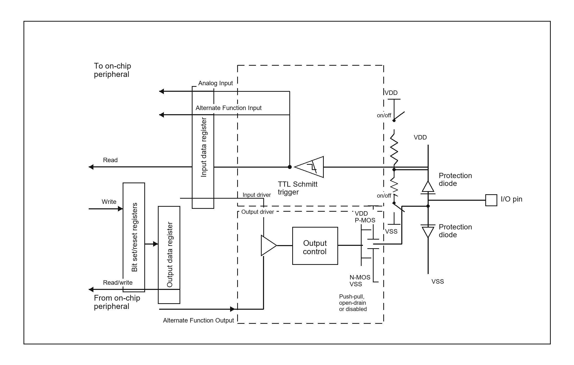
This chapter keeps the GPIO chapter in a reference-manual style. Package pin and alternate-function facts remain in Section 5, while the mode figures below stay focused on the internal port-bit structure reconstructed from RM0008.
2 Main features
- 16 independently programmable port bits
- Input mode: analog, floating input, pull-up / pull-down input
- Output mode with programmable maximum speed: 10 MHz, 2 MHz, or 50 MHz
- Output structure: push-pull or open-drain
- Alternate-function output mode for timer, communication, and peripheral signals
- Input data sampling through GPIOA_IDR
- Output latch read/write through GPIOA_ODR
- Atomic bit set/reset through GPIOA_BSRR
- Optional reset-only path through GPIOA_BRR
- Configuration lock through GPIOA_LCKR
4 I/O port bit configuration
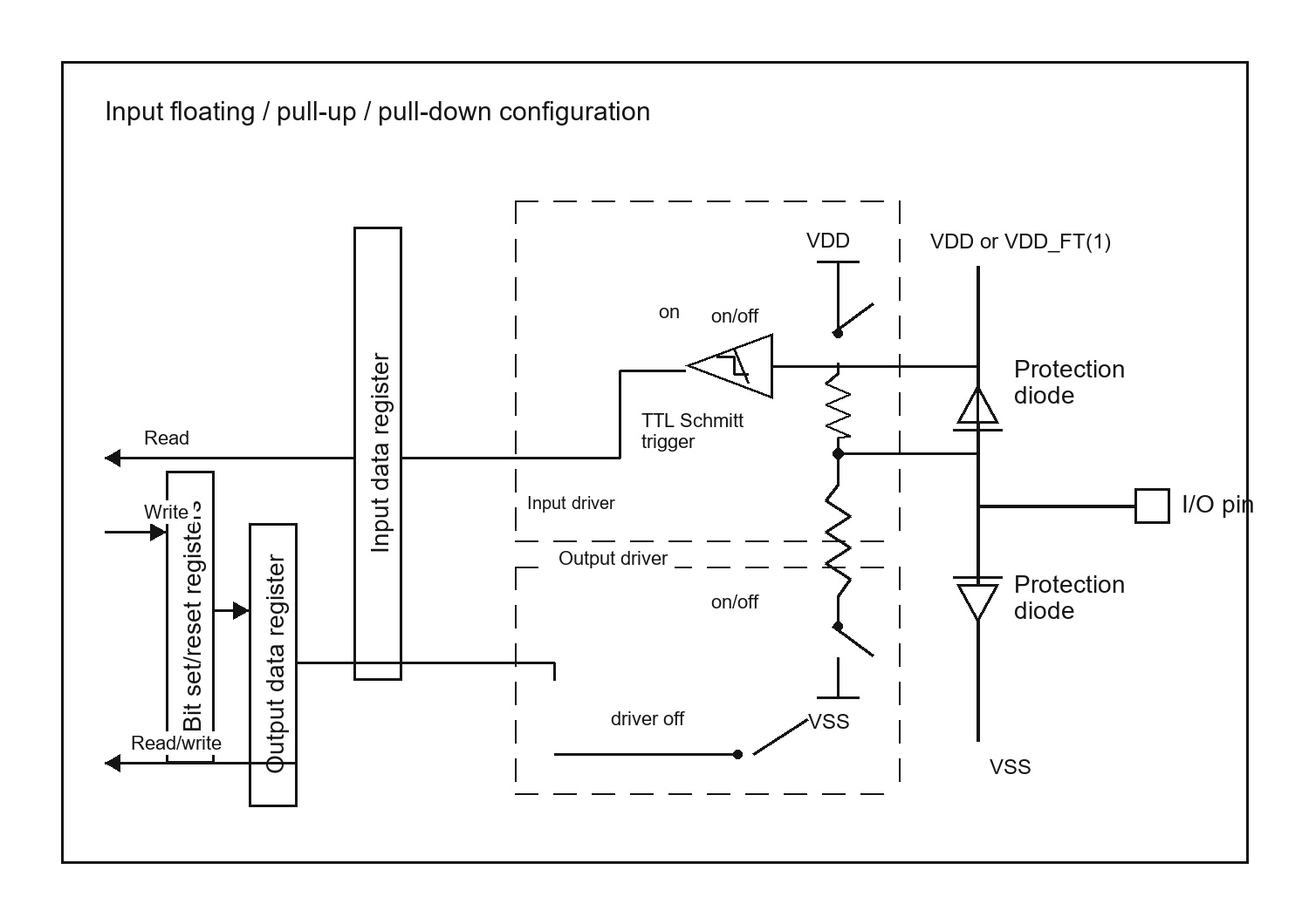
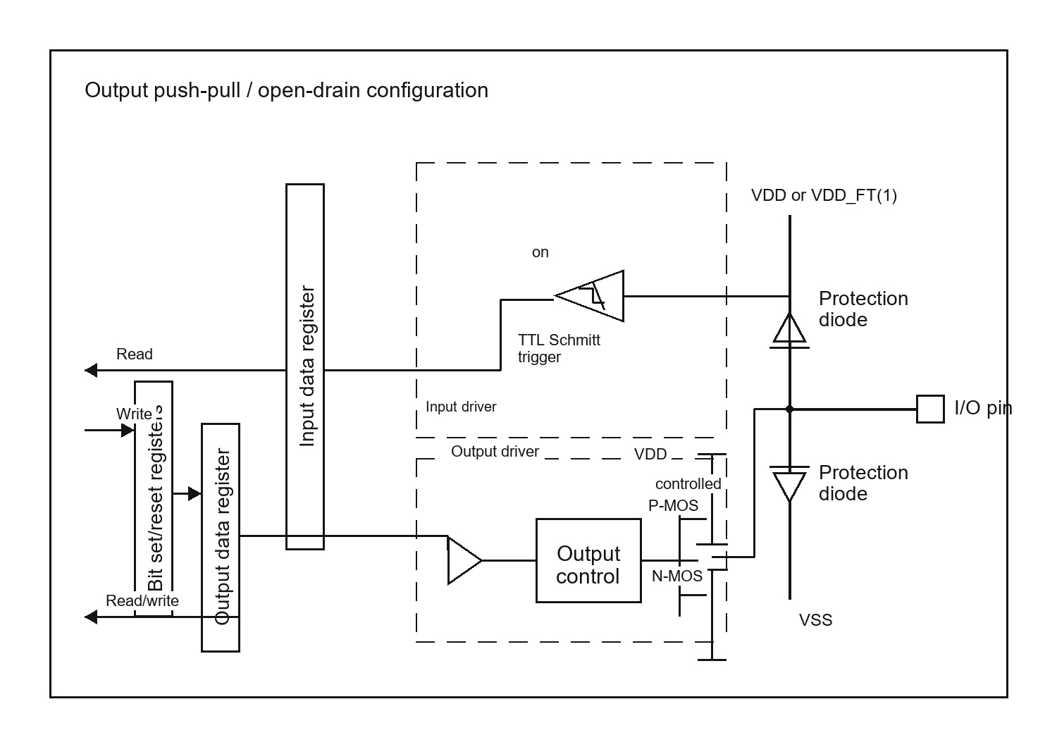
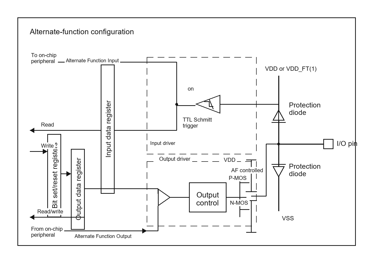
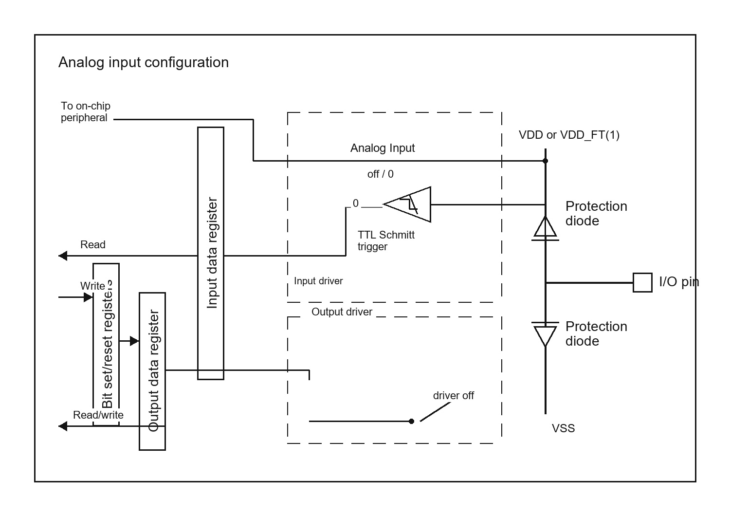
These figures were redrawn from RM0008 Figure 13 through Figure 18 and intentionally keep a vendor-style black-and-white technical tone. They show the internal one-bit GPIO path selected by MODE/CNF; they are not trainer-board wiring diagrams. Trainer-specific routes are documented in Section 8.
4.1 How to read Figures 2-5
| Figure |
What it proves |
Register path to look for |
Current trainer example |
| Figure 2 input |
The pad is sampled through the Schmitt input path; the output driver is disconnected. |
GPIOx_CRL/CRH input mode -> GPIOx_IDR bit y; for this chapter, x=A, so y=5 means PA5 / GPIOA_IDR bit5 |
PA5 / FAULT_IN, PA6 / HALL_IN |
| Figure 3 output |
The output latch and output driver control the pad; the input path can still sample the pad level. |
GPIOx_CRL/CRH output mode -> GPIOx_ODR/BSRR/BRR bit y; for example x=A, y=3 means PA3 / GPIOA_ODR bit3 |
PA3 / DRV_EN, PA4 / DRV_DIR; PB0 / STATUS_LED and PB1 / USER_OUT are GPIOB quick-route examples in Section 8.5 |
| Figure 4 alternate function |
An on-chip peripheral owns the input/output path instead of plain GPIO software writes. |
GPIOx_CRL/CRH alternate-function mode -> AF input/output peripheral path; official PA2 timer function is TIM2_CH3 |
PA2 / PWM_OUT trainer route is documented in the TIM2 chapter; official PA2 timer function is TIM2_CH3, so this is not a full GPIOA-owned PWM mux |
| Figure 5 analog |
The analog pad path is active; the digital input buffer and output driver are disabled, so IDR reads as 0 on real STM32 behavior. |
GPIOx_CRL/CRH analog mode -> ADC channel path, plus ADC clock/conversion setup; current trainer example PA1 / GPIOA_CRL[7:4] / ADC1_IN1 |
PA1 / ADC1_IN1 / CURRENT_SENSE |
4.2 Configuration bit meaning
| MODE[1:0] |
CNF[1:0] |
Mode |
Description |
| 00 |
00 |
Input / analog |
Analog input mode. Digital input path disabled. |
| 00 |
01 |
Input / floating |
Floating digital input. |
| 00 |
10 |
Input / pull-up-down |
Pull direction selected by the corresponding ODR bit. |
| 01, 10, 11 |
00 |
Output push-pull |
General-purpose push-pull output. |
| 01, 10, 11 |
01 |
Output open-drain |
General-purpose open-drain output. |
| 01, 10, 11 |
10 |
AF push-pull |
Alternate-function push-pull output. |
| 01, 10, 11 |
11 |
AF open-drain |
Alternate-function open-drain output. |
4.3 Output speed encoding
| MODE[1:0] |
Meaning |
Notes |
| 00 |
Input mode |
No output driver speed selection. Input behavior is determined by CNF. |
| 01 |
Output mode, max speed 10 MHz |
General-purpose or alternate-function output, depending on CNF. |
| 10 |
Output mode, max speed 2 MHz |
Frequently used for ordinary control outputs where high edge rate is not required. |
| 11 |
Output mode, max speed 50 MHz |
Highest output transition capability. Use only when signal timing or peripheral function requires it. |
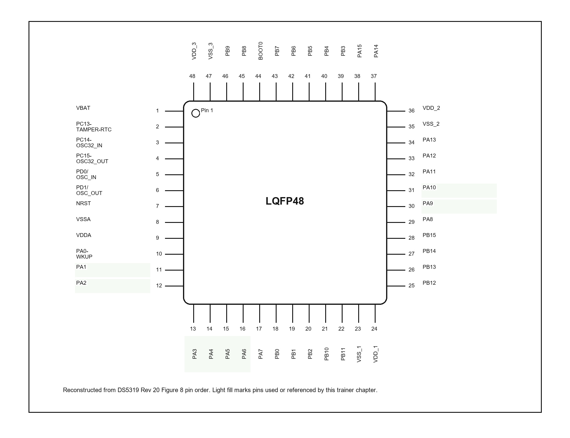
5 Package pinout and pin definitions
Real STM32 datasheets do not start pin study from GPIO registers. They first show a package pinout and a pin-definition
table. From that table, the reader identifies the package pin, the pad name, the pad type, and the alternate peripheral
name. Register lookup then moves to the relevant reference-manual chapter: GPIO, RCC, ADC, TIM, EXTI, or USART.
5.1 Datasheet-style pin definition excerpt
The table below follows the logic of the STM32F103 pin-definition table, but it is intentionally a local reference
excerpt rather than the full ST alternate-function list. The Type and
I/O level columns answer whether the physical pad can be used as GPIO. The
documented-function column only names routes that connect to another HTML chapter in this site. Read the final column in a fixed order:
GPIO register inference first, then the owning local chapter, then the current trainer result.
| LQFP48 pin |
Pin name |
Type |
I/O level |
Main function after reset |
Locally documented function / route |
Register inference / owning chapter / current result |
| 10 |
PA0-WKUP |
I/O |
- |
PA0 |
TIM2_CH1_ETR |
GPIO register inference: PA0 -> GPIOA_CRL[3:0] and GPIO data bit 0. Owning chapter: official TIM2_CH1_ETR pin truth is in TIM2 PWM Datasheet. Current trainer result: no rendered PA0 node; GPIO writes latch only. |
| 11 |
PA1 |
I/O |
- |
PA1 |
ADC1_IN1 |
GPIO register inference: PA1 -> GPIOA_CRL[7:4] and GPIO data bit 1. Owning chapter: PA1 / ADC1_IN1 / CURRENT_SENSE conversion is in ADC1 Datasheet. Current trainer result: visible ADC path uses IOPAEN + ADC1EN + GPIOA_CRL[7:4]=0x0 + ADC1_CR[1] + ADC1_DR_CH1; GPIO output writes latch only. |
| 12 |
PA2 |
I/O |
- |
PA2 |
TIM2_CH3 |
GPIO register inference: PA2 -> GPIOA_CRL[11:8] and GPIO data bit 2. Official pin truth: PA2 = TIM2_CH3 on STM32F103. Owning chapter: timer behavior for the PA2 / PWM_OUT trainer route is in TIM2 PWM Datasheet. Current trainer result: visible PWM uses IOPAEN + TIM2EN + GPIOA_CRL[11:8] + TIM2_CCER[0] + TIM2_CCR1; this is a trainer route, not full TIM2 channel muxing. |
| 13 |
PA3 |
I/O |
- |
PA3 |
GPIO output |
GPIO register inference: PA3 -> GPIOA_CRL[15:12] and GPIOA_ODR/BSRR/BRR bit 3. Owning chapter: local GPIO output route PA3 / DRV_EN. Current trainer result: visible output when IOPAEN is set, output mode is selected, and bit 3 is written. |
| 14 |
PA4 |
I/O |
- |
PA4 |
GPIO output |
GPIO register inference: PA4 -> GPIOA_CRL[19:16] and GPIOA_ODR/BSRR/BRR bit 4. Owning chapter: local GPIO output route PA4 / DRV_DIR. Current trainer result: visible output when IOPAEN is set, output mode is selected, and bit 4 is written. |
| 15 |
PA5 |
I/O |
- |
PA5 |
GPIO input |
GPIO register inference: PA5 -> GPIOA_CRL[23:20] and GPIOA_IDR bit 5. Owning chapter: local GPIO input route PA5 / FAULT_IN. Current trainer result: board-driven active-high input; output writes may latch but do not drive this board input route. |
| 16 |
PA6 |
I/O |
- |
PA6 |
GPIO input / EXTI6 |
GPIO register inference: PA6 -> GPIOA_CRL[27:24] and GPIOA_IDR bit 6. Owning chapter: interrupt edge/pending flow for PA6 / HALL_IN / EXTI6 is in EXTI Datasheet. Current trainer result: fixed board-driven PA6 rising-edge route through AFIOEN + IOPAEN + EXTI_IMR/RTSR/PR; GPIO output-mode writes latch only and do not drive HALL_IN. Falling-edge/remap behavior is reference-only. |
| 30 |
PA9 |
I/O |
FT |
PA9 |
USART1_TX |
GPIO register inference: PA9 -> GPIOA_CRH[7:4] and GPIO data bit 9. Owning chapter: USART1_TX behavior is in USART1 Datasheet. Current trainer result: USART1_DR writes appear as a TX log effect when USART1 is enabled; no separate PA9 board wire is rendered. |
| 31 |
PA10 |
I/O |
FT |
PA10 |
USART1_RX |
GPIO register inference: PA10 -> GPIOA_CRH[11:8] and GPIO data bit 10. Owning chapter: PA10 / USART1_RX / COMM_RX behavior is in USART1 Datasheet. Current trainer result: External Comm drives the fixed RX route through USART1_SR.RXNE and USART1_DR when receive is enabled. |
5.2 How PA1 maps to registers
Example: PA1 is a package pad whose type is I/O, so it can be GPIO
on the real STM32F103. Because the pin number inside the port is 1, GPIO configuration lives in
GPIOA_CRL bits [7:4]. If the selected function is
ADC1_IN1, the GPIO chapter only gives the pad-side analog mode; the ADC chapter owns
RCC_APB2ENR.ADC1EN, ADC1_CR, and
ADC1_DR_CH1.
The same rule applies across the table: PA0..PA7 use
GPIOA_CRL, PA8..PA15 use
GPIOA_CRH, port output uses ODR/BSRR/BRR, port input uses
IDR, locally documented ADC names go to the ADC chapter, timer names go to the TIM chapter, USART names
go to the USART chapter, and interrupt use of a GPIO line goes through AFIO/EXTI.
Datasheet reading rule: entries whose type column is I/O and whose I/O level is blank or FT
are GPIO-capable package pads before a peripheral route claims the pad. Supply, reset, boot, oscillator-only, and power-reference rows are not treated as ordinary GPIO.
Rows not listed in this local excerpt are official-reference behavior or register-latch-only unless another local peripheral chapter owns a trainer route.
Important distinction: on STM32F103-style pin rows, Type = I/O means the silicon pad is a bidirectional GPIO-capable pad.
GPIO input-only behavior usually comes from the selected register mode, board wiring, or a trainer route such as
PA5 / FAULT_IN, not from the I/O type itself. Rows typed as supply, reset, boot,
oscillator-only, or other special-function-only pins should not be tested as ordinary GPIO outputs.
6 Register map and reset values
| Offset |
Register |
Reset value |
Description |
| 0x00 |
GPIOA_CRL |
0x44444444 |
Port configuration register low, for pins 0 to 7 |
| 0x04 |
GPIOA_CRH |
0x44444444 |
Port configuration register high, for pins 8 to 15 |
| 0x08 |
GPIOA_IDR |
0x00000000 |
Port input data register |
| 0x0C |
GPIOA_ODR |
0x00000000 |
Port output data register |
| 0x10 |
GPIOA_BSRR |
0x00000000 |
Port bit set/reset register |
| 0x14 |
GPIOA_BRR |
0x00000000 |
Port bit reset register |
| 0x18 |
GPIOA_LCKR |
0x00000000 |
Port configuration lock register |
7 Register descriptions
7.1 Port configuration low register (GPIOA_CRL)
Address offset: 0x00
Reset value: 0x44444444
Bits 31:0 Each pin uses four configuration bits arranged as CNFy[1:0] and
MODEy[1:0]. Pins y = 0..7 are described in GPIOA_CRL.
In this GPIOA chapter, y is the A-port pin number:
y=0 -> PA0 / GPIOA_CRL[3:0],
y=1 -> PA1 / GPIOA_CRL[7:4],
y=3 -> PA3 / GPIOA_CRL[15:12], and so on.
7.2 Port configuration high register (GPIOA_CRH)
Address offset: 0x04
Reset value: 0x44444444
Bits 31:0 Same format as GPIOA_CRL, but applied to pins
y = 8..15. In this chapter, y=10 means
PA10 / GPIOA_CRH[11:8].
7.3 Port input data register (GPIOA_IDR)
Address offset: 0x08
Reset value: 0x00000000
Bits 15:0 IDRy: These bits are read-only and return the sampled logic state present on the corresponding I/O
pin. A read of GPIOA_IDR returns the current port input level regardless of whether the output latch
contains a different value. In this chapter, IDR5 means PA5 / FAULT_IN
and IDR6 means PA6 / HALL_IN.
7.4 Port output data register (GPIOA_ODR)
Address offset: 0x0C
Reset value: 0x00000000
Bits 15:0 ODRy: These bits can be read and written by software. When a pin is configured as a general-purpose or
alternate-function output, ODRy provides the output latch value. For atomic updates, use
GPIOA_BSRR. In this chapter, ODR3 means
PA3 / DRV_EN and ODR4 means PA4 / DRV_DIR.
7.5 Port bit set/reset register (GPIOA_BSRR)
Address offset: 0x10
Reset value: 0x00000000
Bits 31:16 BRy: Writing 1 resets the corresponding ODRy bit.
Bits 15:0 BSy: Writing 1 sets the corresponding ODRy bit.
For example, BS3 sets PA3 / DRV_EN high and
BR4 resets PA4 / DRV_DIR low.
In the official RM0008 model, set has priority if both halves target the same bit in one access. The current simulator applies
the set mask first and then the reset mask, so the trainer-observable tie case behaves as reset-wins.
7.6 Port bit reset register (GPIOA_BRR)
Address offset: 0x14
Reset value: 0x00000000
Writing a 1 to BRy clears the corresponding ODRy bit. This register provides a
reset-only path similar to the upper half of GPIOA_BSRR. For this chapter,
BR3 clears PA3 / DRV_EN and
BR4 clears PA4 / DRV_DIR.
7.7 Port configuration lock register (GPIOA_LCKR)
Address offset: 0x18
Reset value: 0x00000000
After the lock key writing sequence, selected configuration bits cannot be modified until the next reset in the official
STM32F103 GPIO model. This mechanism is used when accidental changes to I/O configuration must be prevented during runtime.
The register is kept in the documentation because it is part of the STM32F103 GPIO surface, but the current trainer does not enforce a hard write lock on GPIOA_CRL or GPIOA_CRH after the sequence.
8 Student register guide and code examples
8.1 Quick first practice path
If a student opens this chapter first, the easiest starting exercise is simple: turn on one visible GPIO output, confirm which
register bit moved, then compare that with one input route and one ADC-related route. The chapter should read like a map from pin
table to register write to visible proof in the site.
| Try this first |
Write in code |
Check in UI |
What it teaches |
| Visible GPIO output |
Enable IOPAEN or IOPBEN, set the output nibble in GPIOA_CRL or GPIOB_CRL, then write the matching ODR/BSRR/BRR bit. |
Register: clock bit, mode nibble, data bit. Pin: DRV_EN, DRV_DIR, STATUS_LED, or USER_OUT. Graph: the same line voltage. |
Clock + mode + data write all matter before the output becomes visible. |
| Board-driven digital input |
Keep PA5 or PA6 in input mode and read GPIOA_IDR; if output mode is selected, the trainer keeps these board routes input-driven and only latches the GPIO write. |
Pin: FAULT_IN or HALL_IN. Register: GPIOA_IDR and, for Hall, the EXTI path. |
Some trainer-visible lines are read paths, not student-driven output paths. |
| PA1 as ADC-side GPIO preparation |
Set GPIOA_CRL[7:4] = 0x0 for analog mode, then continue with ADC1_CR in the ADC chapter. |
Register: PA1 nibble, ADC enable bit, and ADC1_DR_CH1 raw value. Pin: CURRENT_SENSE. Graph: PA1 / CURRENT_SENSE voltage trace. |
PA1 is GPIO-capable in the pin table, but the current trainer exposes it as a visible ADC route rather than a visible GPIO output. |
| Code-to-UI proof |
Use watch_u32() for named values and read/write the mapped trainer registers directly. |
Watch / Access for watched values and register reads/writes alongside Register, Pin, and Graph. |
The same chapter should let the student explain both the register write and the visible result. |
8.2 Input configuration sequence
- Enable the GPIOA peripheral clock first through RCC->APB2ENR.
- Select input mode by writing MODEy = 00; for PA5, this is MODE5 in GPIOA_CRL[23:20].
- Select analog, floating, or pull-up/down behavior through CNFy; for PA6, this is CNF6 in GPIOA_CRL[27:24].
- For pull-up/down input mode, program the corresponding ODRy bit to choose pull direction, such as ODR5 for PA5.
- Read the current logic level through GPIOA_IDR.
8.3 Output configuration sequence
- Enable the GPIOA peripheral clock through RCC->APB2ENR.
- Also enable AFIOEN when the route is used together with EXTI source selection or alternate-function setup guidance from another chapter.
- Select output speed through MODEy; for PA3 / DRV_EN, this is MODE3 in GPIOA_CRL[15:12].
- Select push-pull, open-drain, alternate-function push-pull, or alternate-function open-drain through CNFy; for PA4 / DRV_DIR, this is CNF4 in GPIOA_CRL[19:16].
- Use GPIOA_BSRR for atomic bit control.
- Use GPIOA_ODR if a full latch write is intended.
8.4 Practical notes
- A read of GPIOA_ODR returns the latched output data, not necessarily the external pin level under all conditions.
- A read of GPIOA_IDR returns the sampled input level at the pad.
- Analog mode should be used for ADC-connected pins to disable the digital input path and reduce unnecessary digital switching.
- For PA1 / CURRENT_SENSE, GPIO analog mode is only the pad-side prerequisite. Actual ADC conversion also needs RCC->APB2ENR.ADC1EN and the ADC-side flow described in the ADC chapter.
- PA1 / CURRENT_SENSE is the visible ADC-gated route in the current trainer; configuring it as a GPIO output changes only the GPIO latch, not the rendered current-sense signal.
- PA5 / FAULT_IN and PA6 / HALL_IN remain board-driven inputs in the current trainer even if GPIOA_CRL selects an output mode.
- For interrupt-driven digital inputs, configure the pin as input and use the external interrupt controller separately.
- Alternate-function outputs still require correct GPIO pin mode in CRL/CRH even when the waveform source comes from a timer or communication peripheral. The peripheral clock on the timer or communication block must also be enabled separately.
- In the current trainer, named GPIO outputs stay at 0 V until the matching APB2 clock bit is enabled and the pin mode is set to output.
- If a student configures the wrong path, the UI usually explains the mismatch in plain detail text such as GPIOA clock gated / 0.00 V, Pin mode is not output / 0.00 V, or output writes latch only.
- For first-pass proof, read the chapter with the site views in this order: Register for clock and mode truth, Pin for direction and register source, Graph for the visible trace, and Watch / Access for watched values and register reads/writes.
- The current motor-driver lab named routes are PA1 / CURRENT_SENSE, PA2 / PWM_OUT, PA3 / DRV_EN, PA4 / DRV_DIR, PA5 / FAULT_IN, and PA6 / HALL_IN. UART and PA0 speed feedback are outside this first-review motor lab map.
// Example 1: configure PA3 as general-purpose push-pull output
RCC->APB2ENR |= (1u << 2);   // IOPAEN
GPIOA->CRL &= ~(0xFu << (3 * 4));
GPIOA->CRL |=  (0x2u << (3 * 4)); // MODE3=10 (2 MHz), CNF3=00 (GP push-pull)
GPIOA->BSRR = (1u << 3);          // set PA3
GPIOA->BSRR = (1u << (16 + 3));   // reset PA3

// Example 2: configure PA6 as floating input
GPIOA->CRL &= ~(0xFu << (6 * 4));
GPIOA->CRL |=  (0x4u << (6 * 4));
if (GPIOA->IDR & (1u << 6)) {
    // PA6 input state is HIGH
}
위 예시는 특정 응용회로를 전제로 하지 않는 GPIO 사용 예시입니다. 실제 제품에서는 같은 방식으로 LED, 드라이버 enable, Hall signal, 버튼, 통신 핀 등을
각각의 포트 비트에 매핑해 사용합니다.
Peripheral clock enable에 대한 상세 설명은 별도 문서 RCC Clock Control Datasheet를 참고합니다.
The PA1 / CURRENT_SENSE analog flow continues in the separate ADC1 Datasheet as
IOPAEN -> ADC1EN -> ADCCLK -> analog mode -> conversion.
8.5 Current trainer GPIO connection map and GPIOB quick routes
Read each GPIO route in this order: pin-definition evidence first, then the RCC gate, then the GPIO configuration field,
then the data register, then the visible board or UI signal. A pin is GPIO-capable in the STM32-style document when its
package row is an I/O pad and its main reset function is the same port name, such as
PA3 or PB0.
The PB0/PB1 rows below are included only as a GPIOB quick-route appendix for visible trainer outputs;
they do not imply ownership by the GPIOA register block.
| Pin or route |
Datasheet I/O type |
Official GPIO use |
Representative alternate functions |
Currently simulated |
Trainer code result |
| PA0 |
I/O |
GPIO-capable pad on the STM32F103 package row. |
TIM2_CH1_ETR |
No rendered PA0 board node in the current trainer. |
GPIO writes latch in the register model only. |
| PA1 / CURRENT_SENSE |
I/O |
GPIO-capable pad; analog mode is selected for ADC use. |
ADC1_IN1 |
PA1 / ADC1_IN1 / CURRENT_SENSE |
CURRENT_SENSE remains ADC-gated; GPIO output writes latch only. |
| PA3 / PA4 |
I/O |
GPIO output-capable pads. |
General-purpose GPIO routes in this local excerpt. |
DRV_EN and DRV_DIR |
Visible Pin View output when IOPAEN, output mode, and data bit writes are present. |
| PA5 / PA6 |
I/O |
GPIO input-capable pads. |
PA6 can feed EXTI6. |
FAULT_IN and HALL_IN / EXTI6 |
Board-driven input paths update GPIOA_IDR; output-mode writes latch only and do not drive FAULT_IN or HALL_IN. PA6 can raise the modeled Hall interrupt. |
| PB0 / PB1 GPIOB quick routes |
I/O |
GPIO output-capable pads on port B. |
General-purpose GPIOB quick routes in this local excerpt. |
STATUS_LED and USER_OUT |
Visible Pin View output when IOPBEN, output mode, and data bit writes are present. |
| Trainer signal |
Pin-definition evidence |
RCC gate |
GPIO mode field |
Data register path |
Connected board/UI result |
| PA3 / DRV_EN |
PA3 row: Type = I/O, reset function PA3, local route GPIO output. |
RCC->APB2ENR.IOPAEN, bit 2, mask 0x00000004. |
GPIOA_CRL[15:12]; output test uses MODE3 != 00 and CNF3 = 00. |
GPIOA_ODR, GPIOA_BSRR, or GPIOA_BRR bit 3. |
Pin View DRV_EN; feeds the motor-driver enable input. |
| PA4 / DRV_DIR |
PA4 row: Type = I/O, reset function PA4, local route GPIO output. |
RCC->APB2ENR.IOPAEN, bit 2, mask 0x00000004. |
GPIOA_CRL[19:16]; output test uses MODE4 != 00 and CNF4 = 00. |
GPIOA_ODR, GPIOA_BSRR, or GPIOA_BRR bit 4. |
Pin View DRV_DIR; feeds the motor-driver direction input. |
| PA5 / FAULT_IN |
PA5 row: Type = I/O, reset function PA5, local route GPIO input. |
RCC->APB2ENR.IOPAEN, bit 2, mask 0x00000004. |
GPIOA_CRL[23:20]; input test uses MODE5 = 00. |
GPIOA_IDR bit 5. |
Pin View FAULT_IN; board-conditioned active-high driver fault input. Selecting output mode in GPIOA_CRL leaves this as a board-driven input route; GPIO writes latch only. |
| PA6 / HALL_IN / EXTI6 |
PA6 row: Type = I/O, reset function PA6, local route GPIO input / EXTI6. |
RCC->APB2ENR.AFIOEN bit 0 plus IOPAEN bit 2. |
GPIOA_CRL[27:24]; input test uses MODE6 = 00. |
GPIOA_IDR bit 6 and the EXTI path EXTI_IMR/RTSR/PR. |
Pin View HALL_IN; Graph View PA6 / HALL_IN. Selecting output mode in GPIOA_CRL leaves this as a board-driven input route; GPIO writes latch only. |
| PB0 / STATUS_LED |
PB0 is an STM32F103 package I/O pad on GPIOB; current trainer maps it to a visible GPIOB output. |
RCC->APB2ENR.IOPBEN, bit 3, mask 0x00000008. |
GPIOB_CRL[3:0]; output test uses MODE0 != 00 and CNF0 = 00. |
GPIOB_ODR, GPIOB_BSRR, or GPIOB_BRR bit 0. |
Pin View STATUS_LED; Board schematic exposes PB0 as a left-side MCU pin for the same visible output test route. |
| PB1 / USER_OUT |
PB1 is an STM32F103 package I/O pad on GPIOB; current trainer maps it to a visible GPIOB output. |
RCC->APB2ENR.IOPBEN, bit 3, mask 0x00000008. |
GPIOB_CRL[7:4]; output test uses MODE1 != 00 and CNF1 = 00. |
GPIOB_ODR, GPIOB_BSRR, or GPIOB_BRR bit 1. |
Pin View USER_OUT; Board schematic exposes PB1 as a left-side MCU pin for the same visible output test route. |
GPIOA peripheral register description
GPIOA-DS001 Rev 1.2